Tuesday, April 30, 2013

1 5 35 Volt DC Regulated Power Supply

Here is the circuit diagram of regulated power supply. It is a small power supply that provides a regulated voltage, adjustable between 1.5 and 35 volts at 1 ampere. This circuit is ready to use, you just need to add a suitable transformer. This circuit is thermal overload protected because the current limiter and thermal overload protection are included in the IC.

Picture of the circuit:
 1A 1.5 volt to 35 volt dc Regulated Power Supply Circuit Schematic
1A Regulated Power Supply Circuit Schematic
 
Circuit diagram:
 1A 1.5 volt to 35 volt dc Regulated Power Supply Circuit Diagram
1A Regulated Power Supply Circuit Diagram
 
Transformer selection chart:
  Transformer Selection Chart for 1A 1.5 volt to 35 volt dc Regulated Power Supply Circuit Diagram
Transformer selection Guide-Table For Power Supply
 
Parts:
IC = LM317
P1 = 4.7K
R1 = 120R
C1 = 100nF - 63V
C2 = 1uF - 35V
C3 = 10uF - 35V
C4 = 2200uF - 35V
D1-D4 = 1N4007

Features:
  • Just add a suitable transformer (see table)
  • Great to power your projects and save money on batteries
  • Suitable as an adjustable power supply for experiments
  • Control DC motors, low voltage light bulbs, …
Specifications :
  • Preset any voltage between 1.5 and 35V
  • Very low ripple (80dB rejection)
  • Short-circuit, thermal and overload protection
  • Max input voltage : 28VAC or 40VDC
  • Max dissipation : 15W (with heatsink)
  • Dimensions : 52x52mm (2.1” x 2.1”)
Technical Specifications
  • Input Voltage = 40Vdc max Transformer
  • Output Voltage = 1.5V to 35Vdc
  • Output Current = 1.5 Amps max.
  • Power Dissipation = 15W max (cooled)
Note:
  • It has not to be cooled if used for small powers. 28 Volt AC max is allowed for the input voltage.
Read More..

Sunday, April 21, 2013

Ampere or Current Booster

Small and very useful circuit, Can be built on a veroboard

Volt regulators such as the LM708, and LM317 series (and others) sometimes need to provide a little bit more current then they actually can handle. If that is the case, this little circuit can help out. A power transistor such as the 2N3772 or similar can be used.

The power transistor is used to boost the extra needed current above the maximum allowable current provided via the regulator.
Current up to 1500mA(1.5amp) will flow through the regulator, anything above that makes the regulator conduct and adding the extra needed current to the output load. It is no problem stacking power transistors for even more current. (see diagram). Both regulator and power transistor must be mounted on an adequate heatsink.

Circuit diagram:
Ampere or Current Booster Circuit Diagram

Parts:

R1 = 1R-2W
R2 = 10R-2W
C1 = 35v-470uF
C2 = 35v-470uF
Q1 = TIP2955
IC1 = 78xx Regulator


Source :http://www.ecircuitslab.com
Read More..

Saturday, April 13, 2013

Mains Manager

Very regularly we omit to change off the peripherals like screen, scanner, and printer while switching off our PC. The problem is that there are separate power switches to show the peripherals off. Normally, the peripherals are related to a single of these four-way trailing sockets that are plugged into a single wall socket. If that socket is obtainable, all the tools may be swaped off from there and none of the equipment used will require any change. 

Here is a majors supervisor circuit that lets you flip all of the tools on or off via just running the swap on any probably the most softwares; as an instance, whilst you switch off your PC, the monitor in addition to different gear will get powered down automatically. You could select the primary tools to keep watch over different devices. 

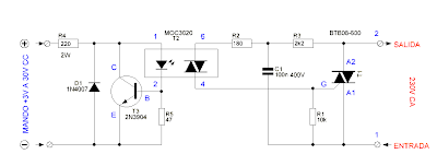
The main gear is to be straight away plugged into the grasp socket, while all other equipment are to be related via the slave socket. The primarys provide from the wall socket is to be linked to the input of the mains manager circuit. The unit functions by sensing the current drawn through the control tools/load from the master socket. On sensing that the keep a watch on equipment is on, it powers up the opposite (slave) sockets.

The load on the master socket can be anyplace between 20 VA and 500 VA, whereas the burden on the slave sockets can be 60 VA to 1200 VA. During the positive half of cycle of the primarys AC supply, diodes D4, D5, and D6 have a voltage drop of about 1.8 volts when present is drawn from the master socket. Diode D7 carries the current all the way in which through negative 1 of 2 cycles. Capacitor C3, in series with diode D3, is hooked up throughout the diode mixture of D4 thru D6, along with diode D7 in addition to resistor R10. Thus current pulses all the highest way thru constructive 1 of 2-cycles, charge up the capacitor to 1.8 volts by implys of diode D3. 

This voltage is enough to carry transistor T2 in forward biased situation for about 200 ms even after the controlling load on the grasp socket is swaped off. When transistor T2 is ‘on’, transistor T1 gets ahead biased and that is swaped on. This, in turn, triggers Triac 1, which then energys the slave hundreds. Capacitor C4 and resistor R9 kind a snubber community to ensure that the triac flips off cleanly with an inductive load.

Circuit diagram:

Mains Manager Circuit Diagram

LED1 point outs that the unit is working. Capacitor C1 and zener ZD1 are successfully in collection across the principles. The resulting 15V pulses across ZD1 are rectified through diode D2 and smoothened via capacitor C2 to present the essential DC provide for the circuit round transistors T1 and T2. Resistor R3 is used to restrict the changeing-on surge current, while resistor R1 serves as a bleeder for unexpectedly discharging capacitor C1 when the unit is unplugged. LED1 glows whenever the unit is plugged into the primarys. Diode D1, in anti-parallel to LED1, carries the current throughout the opposite half of cycles. Don’t plug the rest into the grasp or slave sockets with out testing the unit.

If that that you may simply assume of, plug the unit into the principles via an earth leakage circuit breaker. The mains LED1 will have to glow and the slave LED2 must stay off. Now join a desk lamp to the grasp socket and switch it ‘on’. The lamp should operate as common. The slave LED must flip ‘on’ each time the lamp plugged into slave socket is changeed on. Both lamps should be at full brightness with none flicker. If so, the unit is working appropriately and may additionally be put into use.

Note:
  1. The device linked to the master socket should have its energy swap on the first facet of the inner transformer. Some electronic tools have the ability swap on the secondary facet and hence these softwares continue to draw a small present from the primarys even when swaped off. Thus such instruments, if connected because the master, is no longer going to control the slave devices appropriately. 
     
  2. Though this unit put offs the energy from the tools being keep a watch onled, it doesn’t provide isolation from the primarys. So, before working inside any equipment related to this unit, it should be unplugged from the socket.


http://www.ecircuitslab.com/2011/05/mains-manager.html
Read More..

Low Power LED Battery Voltmeter Schematic


This is a low power voltmeter circuit that can be used with alternative energy systems that run on 12 and 24 volt batteries. The voltmeter is an expanded scale type that indicates small voltage steps over the 10 to 16 volt range for 12 volt batteries and over the 22 to 32 volt range for 24 volt batteries. Power consumption can be as low as 14mw when operated from 12V and 160mw when operated from 24V. It is possible to set the meter to read equal steps across a variety of upper and lower voltages. The meter saves power by operating in a low duty-cycle blinking mode where the LED indicators are only on and consuming power briefly during a repeating 2 second cycle. The circuit may be switched to a high power mode where the active LED stays on at all times.

Different colored LEDs may be used for the voltage level indicator, this allows the battery state to be read in the dark. With the new blue LEDs, it is possible to have a nice looking rainbow of colors using two each of red, amber, yellow, green, and blue LEDs. The circuit will also work with inexpensive and common red LEDs. If the circuit is to be used in sunlight, ultra-bright LEDs should be used, although even those may be hard to read without some kind of sun shield. The circuit may be built with either the CMOS ICM7555 timer or the more common bipolar 555 timer. The 7555 timer will provide much more efficient operation and should be used for systems with small batteries.

Theory for 12 Volt operation
The heart of the circuit is the LM3914N dot-bar volt meter IC, U2. This chip is operated in the expanded-scale mode so that the circuit responds in the 10-16V range. U2 outputs a steady voltage on pin 7 from the internal voltage reference. This is fed via voltage dividers VR2 and R5 to the internal reference input pins to set the range that the meter is sensitive to. The measured voltage is fed in on pin 5 via the voltage divider consisting of R4 and VR1. This divider scales the input voltage down to a range that is useful to the IC.

The U2 positive supply is connected to pin 3 which is nominally 12V. The U2 negative supply is switched on momentarily via transistor Q1, this switching action is what makes the circuit efficient since U1 (ICM7555) consumes a mere 0.34 ma while U2 consumes around 18ma with one LED on. The ICM7555 timer, U1 is wired to run in a free-running mode with a narrow pulse width square wave output.

The duty-cycle of U1 is controlled by the ratio of R1 and R2. R2 may be adjusted to a smaller value if faster blinking is desire, a potentiometer may be substituted for R2 if a rate adjustment is desired. R1 may be increased if a longer on-time is desired. Changes in R1 and R2 will affect the average current that the circuit consumes. The frequency of oscillation is determined by C1, R1, and R2. C1 may be either an electrolytic or poly capacitor, if an electrolytic part is used, be sure to connect the positive terminal to U1 pins 6 and 2 and the negative terminal to ground.

The output of the timer IC is fed through current limiting resistor R3 to transistor Q1 which controls power to U2. Capacitor C2 filters the control voltage input to U1 and capacitor C3 provides DC filtering for the whole circuit. When the lock-on switch across capacitor C1 is closed, the output of the timer remains on, thus enabling the U2 circuitry and increasing the current drain to 18mA. The reason the switch is not simply wired across the transistor is to keep the negative supply to U2 the same as when the circuit is pulsed on. This maintains the same calibration on the LEDs in both modes because the transistors voltage drop is always part of the circuit.

Last, but not least, fuse F1 protects against the potential for fire hazard should the circuit become shorted out. The average current is calculated by adding the constant current required by U1 with the product of the current from U2 times the duty cycle, see the specifications for details. To operate the circuit in the 12V mode, wire the circuit so that jumpers J2 and J5 are shorted, parts U3, C4, R6, and R7 may be left out.

Theory for 24 Volt operation
When wired for 24 Volt operations, the meter responds in the 20-32V range. R6 is connected to the 24V supply instead of R4, the greater value of R6 scales the higher input voltage to a range that is useful for U2. Voltage regulator U3 with series resistor R7 scales the 24V down to a regulated 12V to provide the proper operating voltage for the ICs. Resistor R7 assures that the input voltage to the regulator stays well below the 35V absolute maximum specification of the IC. Operation in 24V mode is less efficient than in 12V mode because of the extra power dissipated by the voltage regulator and R7. To operate the circuit in the 24V mode, wire the circuit so that jumpers J1, J3, and J4 are shorted. R4 may be left out in the 24V mode.

Read More..

Friday, April 12, 2013

Long Interval Pulse Generator

A rectangular-wave pulse generator with an especially long period may additionally be constructed the usage of most effective two parts: a National Semiconductor LM3710 supervisor IC and a 100-nF capacitor to do away with noise spikes. This circuit utilises the watchdog and reset timers within the LM3710. The watchdog timer is reset when an facet seems on the WDI enter (pin 4). If WDI is constantly held at floor degree, there are usually not any areas and the watchdog times out. After an interval TB, it triggers a reset pulse with a length TA and is reloaded with its initial price. The cycle then begins all over once more. As a result, pulses with a period of TA + TB are existing on the RESET output (pin 10).

Circuit diagram:
\"long-interval-pulse-generator-circuit-diagram\" Long-Interval Pulse Generator Circuit Diagram

\"long-interval-pulse-generator-diagram\"

As may additionally be viewed from the table, periods ranging as a lot as around 30 2ds may additionally be done on this manner. The two intervals TA and TB are determined by internal timers in the IC, which is available in quite quite a bit of models with 4 completely different varys for every timer. To obtain the specified interval, it's vital to order the fitting version of the LM3710. The type designation is decoded in the accompanying desk. 

The reset threshold voltage is beside the point for this explicit utility of the LM3710. The versions shown in daring face had been to be had on the time of printing. Current information can be found on the manufacturer’s house page (www.national.com). The numbers in brackets point out the minimal and maximum worths of intervals TA and TB for which the LM3710 is tested. The circuit functions with a provide voltage within the vary of 3–5 V.


Author: Gregor Kleine Copyright: Elektor Electronics
Read More..

Temperature Meter

The
use of temperature devices in temperature measurement and sensing have
made tremendous progress in the last few decades. There are a few types
of measurement solutions that you can implement in your projects. The
use of thermistors or thermocouples are the two most widely used devices
in measurement solutions. The recent decade has seen the use of
integrated circuits devices in many temperature control related systems
because they are much smaller, provide a more accurate measurement and
simpler to be integrated to other digital control devices.

Most
of the digital temperature sensor system has a built-in communication
bus to enable it to communicate with the master control IC. The most
used communication interface is called I2C, a simple bi-directional
2-wire bus that was developed by Philips Semiconductors in the 1980s.
Since then, many devices has this built in communication protocol that
enables all devices that have this feature to be linked together without
any other additional components. The I2C interfacing standard has
become a world standard that are used in more than 1,000 integrated
circuits.

The
I2C standard basically define the start, stop, device selection
addressing and data transfer interfacing protocol. The hardware consists
of 2 I/O lines called SDA and SCL lines.

START Condition

The
Start Data Transfer is initiated when there is a change of state of SDA
line from HIGH logic to LOW logic while the SCL line is at HIGH logic.
This is the START condition.
STOP Condition

The
Stop Data Transfer is initiated when there is a change of state of SDA
line from LOW logic to HIGH logic while the SCLline is at HIGH logic.
This is the STOP condition.

DATA Transfer Condition

The
data transfer is done between the START and STOP conditions with the
data being transferred when SCL transition fromLOW to HIGH logic. Data
is read when SCL is at HIGH logic. SDA line data will only change when
SCL line is at LOW logic.There is no limit to the number of data bytes
transferred and is determined by the master device. Acknowledgement of
successful transfer of data is done between the master and the slave
devices at regular interval.

Digital Temperature Sensor Applications

If
you are into designing of thermostat controls for various buildings,
industrial controls or home appliances, you maywant to consider using
the TMP100 digital temperature sensor from Texas Instruments. This
device can be connected tothe microcontroller using the SCL and SDA
lines.

The features of the TMP100 sensor include:

   
* Low Quiescent standby current of 0.1uA means if you choose a proper
microcontroller, the device using battery powered could last for years
compared to the use of thermistor.

    * Temperature range from -55 °C to 125 °C.
    * Wide Power supply range from 2.7V to 5.5V.
    * Accuracy of +/- 2.0 °C.
    * Resolution up to 0.0625 ° C.

The typical application of the TMP100 digital temperature sensor is as shown in the diagram below.

Read More..

Clap Switch Circuit Diagram

Here’s a clap switch free from false triggering. To turn on/off any appliance, you just have to clap twice. The circuit changes its output state only when you clap twice within the set time period. Here, you’ve to clap within 3 seconds. 

The clap sound sensed by condenser microphone is amplified by transistor T1. The amplified signal provides negative pulse to pin 2 of IC1 and IC2, triggering both the ICs. IC1, commonly used as a timer, is wired here as a monostable multivibrator. Trigging of IC1 causes pin 3 to go high and it remains high for a certain time period depending on the selected values of R7 and C3. 

This ‘on’ time (T) of IC1 can be calculated using the following relationship: T=1.1R7.C3 seconds where R7 is in ohms and C3 in microfarads. On first clap, output pin 3 of IC1 goes high and remains in this standby position for the preset time.Also, LED1 glows for this period. The output of IC1 provides supply voltage to IC2 at its pins 8 and 4.
Circuit diagram :
Clap Switch  Circuit Diagram
Clap Switch Circuit Diagram

Now IC2 is ready to receive the triggering signal. Resistor R10 and capacitor C7 connected to pin 4 of IC2 prevent false triggering when IC1 provides the supply voltage to IC2 at first clap. On second clap, a negative pulse triggers IC2 and its output pin 3 goes high for a time period depending on R9 and C5.

 This provides a positive pulse at clock pin 14 of decade counter IC 4017 (IC3). Decade counter IC3 is wired here as a bistable. Each pulse applied at clock pin 14 changes the output state at pin 2 (Q1) of IC3 because Q2 is connected to reset pin 15. The high output at pin 2 drives transistor T2 and also energizes relay RL1. LED2 indicates activation of relay RL1 and on/off status of the appliance. A free-wheeling diode (D1) prevents damage of T2 when relay de-energizes.
 
 
http://streampowers.blogspot.com/2012/06/clap-switch-circuit-diagram.html
Read More..

Automotive Electrical Diagrams Provide Symbols Represent Circuit

Electrical Wiring Diagrams on Free Wiring Diagrams   Download Free Wiring Schematics
Free Wiring Diagrams Download Free Wiring Schematics.


Electrical Wiring Diagrams on Series 600 Electric Wiring Diagram   Car Parts And Wiring Diagram
Series 600 Electric Wiring Diagram Car Parts And Wiring Diagram.


Electrical Wiring Diagrams on Wiring Diagram
Wiring Diagram.


Electrical Wiring Diagrams on Automotive Electrical Diagrams Provide Symbols That Represent Circuit
Automotive Electrical Diagrams Provide Symbols That Represent Circuit.


Electrical Wiring Diagrams on Residential Circuit Diagram Electrical Wiring Information
Residential Circuit Diagram Electrical Wiring Information.


Electrical Wiring Diagrams on 1964 Gmc Truck Electrical System Wiring Diagram   Circuit Schematic
1964 Gmc Truck Electrical System Wiring Diagram Circuit Schematic.


Electrical Wiring Diagrams on Honda Goldwing Gl1100 Wiring Diagram And Electrical System Harness
Honda Goldwing Gl1100 Wiring Diagram And Electrical System Harness.


Electrical Wiring Diagrams on Typical 7 Way Trailer Wiring Diagram   Circuit Schematic
Typical 7 Way Trailer Wiring Diagram Circuit Schematic.


Electrical Wiring Diagrams on Standard Electric Water Heater Operation
Standard Electric Water Heater Operation.


Electrical Wiring Diagrams on Three Way Switch Wiring Diagram
Three Way Switch Wiring Diagram.


Read More..

Solid State Relay Circuit Diagram

Solid State Relay Circuit
Solid state relay is a series that functions like a relay hibryd mechanics. Solid state relays is built with insulating an MOC for separate the input and the switch. With Solid state relays we can avoid the occurrence of sparks as it did in the relay can also avoid the occurrence of conventional connection is not perfect because porous contactor as in conventional relays.


The series of solid state relays This is quite simple and we can make in a PCB hole. For more details can be seen in the picture following a series of solid state relays.

Solid State Relay Circuit
Solid State Relay Circuit Diagram

Solid state relay has many advantages including no mechanical friction on the contactor, the connection process only occur when there are crosses zero, there is no spark at the contactor, not noisy, small konsusi flow control, better endurance.
Read More..

Thursday, April 11, 2013

Modular Phono Preamplifier

High Quality Moving Magnet Pick-up module, Two-stage Series/Shunt feedback RIAA equalization
Any electronics amateur still in possess of a collection of vinyl recordings and aiming at a high quality reproduction should build this preamp and add it to the Modular Preamplifier chain. This circuit features a very high input overload capability, very low distortion and accurate reproduction of the RIAA equalization curve, thanks to a two-stage op-amp circuitry in which the RIAA equalization network was split in two halves: an input stage (IC1A) wired in a series feedback configuration, implementing the bass-boost part of the RIAA equalization curve and a second stage, implementing the treble-cut part of the curve by means of a second op-amp (IC2A) wired in the shunt feedback configuration.

This module comprises also an independent dual rail power supply identical to that described in the Modular Preamplifier Control Center. As with the other modules of this series, each electronic board can be fitted into a standard enclosure: Hammond extruded aluminum cases are well suited to host the boards of this preamp. In particular, the cases sized 16 x 10.3 x 5.3 cm or 22 x 10.3 x 5.3 cm have a very good look when stacked. See below an example of the possible arrangement of the rear panel of this module.

Modular Phono Preamplifier Circuit diagram:
Modular Phono Preamplifier Circuit Diagram

Parts:
R1_____________270R 1/4W Resistor
R2_____________100K 1/4W Resistor
R3_____________2K2 1/4W Resistor
R4_____________39K 1/4W Resistor
R5_____________3K9 1/4W Resistor
R6_____________390K 1/4W Resistor
R7_____________33K 1/4W Resistor
R8_____________75K 1/4W Resistor (or two 150K resistors wired in parallel)
R9_____________560R 1/4W Resistor
C1_____________220pF 63V Polystyrene or Ceramic Capacitor
C2_____________1µF 63V Polyester Capacitor
C3_____________47µF 25V Electrolytic Capacitor
C4_____________10nF 63V Polyester Capacitor 5% tolerance or better
C5_____________1nF 63V Polyester Capacitor 5% tolerance or better
C6,C9__________100nF 63V Polyester Capacitors
C7,C10_________22µF 25V Electrolytic Capacitors
C8,C11_________2200µF 25V Electrolytic Capacitors
IC1____________LM833 or NE5532 Low noise Dual Op-amp
IC2____________TL072 Dual BIFET Op-Amp
IC3____________78L15 15V 100mA Positive Regulator IC
IC4____________79L15 15V 100mA Negative Regulator IC
D1,D2_________1N4002 200V 1A Diodes
J1,J2__________RCA audio input sockets
J3_____________Mini DC Power Socket

Notes:
  • The circuit diagram shows the Left channel only and the power supply
  • Some parts are in common to both channels and must not be doubled. These parts are: IC3, IC4, C6, C7, C8, C9, C10, C11, D1, D2 and J3.
  • IC1 and IC2 are dual Op-Amps, therefore the second half of these devices will be used for the Right channel
  • This module requires an external 15 - 18V ac (50mA minimum) Power Supply Adaptor.
Technical data:
Sensitivity @ 1KHz: 4.3mV RMS input for 200mV RMS output
Max. input voltage @ 100Hz: 53mV RMS
Max. input voltage @ 1KHz: 212mV RMS
Max. input voltage @ 10KHz: 477mV RMS
Frequency response @ 200mV RMS output: flat from 30Hz to 23KHz; -0.5dB @ 20Hz
Total harmonic distortion @ 1KHz and up to 8.8V RMS output: 0.0028%
Total harmonic distortion @10KHz and up to 4.4V RMS output: 0.008%

Source :  http://www.ecircuitslab.com/2011/06/modular-phono-preamplifier.html
Read More..

Soldering Iron Tip Preserver

Although 60/40 solder melts at about 200&degC, the tip temperature of a soldering iron should be at about 370&degC. This is necessary to make a good quick joint, without the risk of overheating delicate components because the iron has to be kept on the joint for too long. Unfortunately, at this temperature, the tip oxidises rapidly and needs constant cleaning. Thats where this circuit can help - it keeps the soldering tip to just below 200&degC while the iron is at rest. Oxidisation is then negligible and the iron can be brought back up to soldering temperature in just a few seconds when needed. In addition, normal soldering operation, where the iron is returned to rest only momentarily, is unaffected because of the thermal inertia of the iron. Two 555 timers (IC1 & IC2) form the heart of the circuit. 

Circuit diagram:
soldering-iron-tip-preserver circuit diagram
Soldering Iron Tip Preserver Circuit Diagram

IC1 is wired as a monostable and provides an initial warm-up time of about 45 seconds to bring the iron up to temperature. At the end of this period, its pin 3 output switches high and IC2 (which is wired in astable configuration) switches the iron on - via relay RLY1 - for about one second in six to maintain the standby temperature. The presence of the iron in its stand is sensed by electrical contact between the two and some slight modification of the stand may be necessary to achieve this. When the iron is at rest, Q1s base is pulled low and so Q1 is off. Conversely, when the iron is out of its stand, Q1 turns on and pulls pins 2 & 6 of IC2 high, to inhibit its operation. During this time, pin 3 of IC2 is low and so the iron is continuously powered via RLY1s normally closed (NC) contacts. Note that the particular soldering iron that the circuit was designed for has its own 24V supply transformer. Other irons may need different power supply arrangements. The warm-up time and standby temperature can be varied by altering R2 and R5, as necessary.


Streampowers
Read More..

Mini Running Text Display

This charming little circuit is a genuine four-digit running-text display, complete with a Christmas / New Year’s greeting. Naturally, any competent programmer can easily arrange to have a different text scroll across the display. The associated soft-ware, including the source code, can be downloaded from the Free Downloads section of our website or obtained from Readers Services on diskette (order number 020365-11).

Mini Running Text Display Circuit Image :
 Simple Mini Running Text Display-Image

As can be seen from the schematic, the hardware consists of little more than an AT90S1200 microcontroller, a 4-digit LED display and a 5-V voltage regulator. The only external circuitry needed by the microcontroller consists of a reset circuit and a 4-MHz crystal, and the remainder of the components are limited to a few decoupling capacitors.

Mini Running Text Display Circuit diagram : 

Simple Mini Running Text Display-Circuit Daigram

In the prototype model, an Osram SLO2016 display module was used. Although this four-digit module measures only 10×20 mm, it provides an especially clear and bright display. In order to give the 7805 voltage regulator sufficient ‘breathing room’, the supply voltage should be at least 8 V. A standard 9-V mains adapter should thus be perfectly adequate. The supply voltage does not have to be stabilised, and the adapter does not have to provide an especially large amount of current, since the running-text display draws scarcely more than 50 mA.

Author : R. van Arem - Copyright : Elektor

Source : http://www.ecircuitslab.com/2012/07/simple-mini-running-text-display.html
Read More..

Information 1990 Pontiac Grand Prixwiring Diagram

Wiring Diagram  Switch on More Information About 1990 Pontiac Grand Prix 3 1l Wiring Diagram
More Information About 1990 Pontiac Grand Prix 3 1l Wiring Diagram.


Wiring Diagram  Switch on Three Way Switch Wiring Diagram
Three Way Switch Wiring Diagram.


Wiring Diagram  Switch on Way Switch Wiring Diagram Variation  3   Electrical Online
Way Switch Wiring Diagram Variation 3 Electrical Online.


Wiring Diagram  Switch on Bridge Humbucker 2 Outer Coils Parallel 3 Both Humbuckers
Bridge Humbucker 2 Outer Coils Parallel 3 Both Humbuckers.


Wiring Diagram  Switch on Way Trailer Wiring Diagram And Connectors Pinout
Way Trailer Wiring Diagram And Connectors Pinout.


Wiring Diagram  Switch on Way Switch Wiring   Electrical   Diy Chatroom   Diy Home
Way Switch Wiring Electrical Diy Chatroom Diy Home.


Wiring Diagram  Switch on Way Power At Switch Diagram
Way Power At Switch Diagram.


Wiring Diagram  Switch on Way Switch Have To Work In Pairs Above Is A Simple Schematic Diagram
Way Switch Have To Work In Pairs Above Is A Simple Schematic Diagram.


Wiring Diagram  Switch on Humbuckers 3 Way Toggle Switch With 1 Volume Guitar Wiring Diagram
Humbuckers 3 Way Toggle Switch With 1 Volume Guitar Wiring Diagram.


Wiring Diagram  Switch on Double Pole Switch Wiring Diagram   Electrical Information Blog   Pc
Double Pole Switch Wiring Diagram Electrical Information Blog Pc.


Read More..

1995 1997 Bmw M3 ABS Wiring Diagram

1995-1997 Bmw M3 ABS Wiring Diagram
(click for full size image)

The Part of  1995-1997 Bmw M3 ABS Wiring Diagram: rear solenoid valve signal, ignition signal, engine control module (DME), auxiliary throttle position sensor, slip control module (ABS), instrument cluster, ABS hydraulic unit ABS brake pedal travel sensor, brake signal, ABS pump motor relay, battery volt, ABS warning indicator,
Read More..

Wednesday, April 10, 2013

Simple Voltmeter Circuit

his circuit provides a simple means to determine the voltage of a low-impedance voltage source. It works as follows. P1, which is a 1-W potentiometer, forms a voltage divider in combination with R1. The voltage at their junction is buffered by T1, and then passed to reference diode D1 via R3. D1 limits the voltage following the resistor to 2.5 V. An indicator stage consisting of T2, R4 and LED D2 is connected in parallel with D1. As long as the voltage is not limited by D1, the LED will not be fully illuminated. This is the basic operating principle of this measurement circuit.
 
Simple Voltmeter Circuit Diagram1
Read More..

Dual 20 Watt Audio Power Amplifier

Overture Audio Power Amplifier Series Dual 20-Watt Audio Power Amplifier with Mute and Standby Modes
The LM1876 is a stereo audio amplifier capable of delivering typically 20W per channel of continuous average output power into a 4 or 8 load with less than 0.1% THD+N. Each amplifier has an independent smooth transition fade-in/out mute and a power conserving standby mode which can be controlled by external logic.

The performance of the LM1876, utilizing its Self Peak Instantaneous Temperature (°Ke) (SPiKe™) protection circuitry, places it in a class above discrete and hybrid amplifiers by providing an inherently, dynamically protected Safe Operating Area (SOA). SPiKe protection means that these parts are safeguarded at the output against overvoltage, undervoltage, overloads, including thermal runaway and instantaneous temperature peaks.

Dual 20-Watt Audio Power Amplifier Circuit diagram :

Dual 20-Watt Audio Power Amplifier

Key Specification
THD+N at 1kHz at 2 x 15W continuous average
output power into 4 or 8: 0.1% (max)
THD+N at 1kHz at continuous average
output power of 2 x 20W into 8: 0.009% (typ)
Standby current: 4.2mA (typ)

Applications :

  • High-end stereo TVs
  • Component stereo
  • Compact stereo
    Features :

  • SPiKe protection
  • Minimal amount of external components necessary
  • Quiet fade-in/out mute mode
  • Standby-mode
  • Isolated 15-lead TO-220 package
  • Non-Isolated 15-lead TO-220 package
  • Wide supply range 20V - 64V 

  • Source : http://www.ecircuitslab.com/2011/06/dual-20-watt-audio-power-amplifier.html
    Read More..

    Boomer Audio Power Amplifier Using LM4906

    The well-known LM386 is an excellent choice for many designs requiring a small audio power amplifier (1-watt) in a single chip. However, the LM386 requires quite a few external parts including some electrolytic capacitors, which unfortunately add volume and cost to the circuit. National Semiconductor recently introduced its Boomer® audio integrated circuits which were designed specifically to provide high quality audio while requiring a minimum amount of external components (in surface mount packaging only). The LM4906 is capable of delivering 1 watt of continuous average power to an 8-ohm load with less than 1% distortion (THD+N) from a +5 V power supply. The chip happily works with an external PSRR (Power Supply Rejection Ratio) bypass capacitor of just 1 µF minimum.

    In addition, no output coupling capacitors or bootstrap capacitors are required which makes the LM4906 ideally suited for cellphone and other low voltage portable applications. The LM4906 features a low-power consumption shutdown mode (the part is enabled by pulling the SD pin high). Additionally, an internal thermal shutdown protection mechanism is provided. The LM4906 also has an internal selectable gain of either 6 dB or 12 dB. A bridge amplifier design has a few distinct advantages over the single-ended configuration, as it provides differential drive to the load, thus doubling output swing for a specified supply voltage. Four times the output power is possible as compared to a single-ended amplifier under the same conditions (particularly when considering the low supply voltage of 5 to 6 volts).

    Boomer Audio Power Amplifier Circuit diagram:


    When pushed for output power, the small SMD case has to be assisted in keeping a cool head. By adding copper foil, the thermal resistance of the application can be reduced from the free air value, resulting in higher PDMAX values without thermal shutdown protection circuitry being activated. Additional copper foil can be added to any of the leads connected to the LM4906. It is especially effective when connected to VDD, GND, and the output pins. A bridge configuration, such as the one used in LM4906, also creates a second advantage over single-ended amplifiers. Since the differential outputs, Vo1 and Vo2, are biased at half-supply, no net DC voltage exists across the load.

    This eliminates the need for an output coupling capacitor which is required in a single supply, single-ended amplifier configuration. Large input capacitors are both expensive and space hungry for portable designs. Clearly, a certain sized capacitor is needed to couple in low frequencies without severe attenuation. But in many cases the speakers used in portable systems, whether internal or external, have little ability to reproduce signals below 100 Hz to 150 Hz. Thus, using a large input capacitor may not increase actual system performance. Also, by minimizing the capacitor size based on necessary low frequency response, turn-on pops can be minimized.

    Source: http://www.ecircuitslab.com/2011/06/boomer-audio-power-amplifier-using.html
    Read More..

    Audio Booster Circuit

    Small and portable unit, Can be built on a veroboard
    The amplifiers gain is nominally 20 dB. Its frequency response is determined primarily by the value of just a few components-primarily C1 and R1. The values of the schematic diagram provide a response of ±3.0 dB from about 120 Hz to better than 20,000 Hz.Actually, the frequency response is ruler flat from about 170 Hz to well over 20,000 Hz; its the low end that deviates from a flat frequency response. 

    The low ends roll-off is primarily a function of capacitor C1(since RIs resistive value is fixed). If C1s value is changed to 0.1 pF, the low ends comer frequency-the frequency at which the low-end roll-off starts-is reduced to about 70 Hz. If you need an even deeper low-end roll-off, change C1 to a 1.0 pF capacitor; if its an electrolytic type, make certain that its installed into the circuit with the correct polarity, with the positive terminal connected to Q1s base terminal.

    Circuit Diagram:
    Audio_Booster_Circuit Diagram 
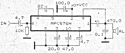
Audio Booster Circuit Diagram

    Parts Description
    P1 100K
    R1 47K
    R2 470K
    R3 10K
    R4 560R
    R5 270R
    C1 0.1uF-25v
    C2 3.3uF-25v
    C3 470uF-25V
    D1 5mm. Red Led
    B1 9v Battery
    J1 RCA Audio Input Socket
    J2 RCA Audio Output Socket
    S1 On-Off Switch


    streampowers
    Read More..

    High and Low Mains Voltage Cut Off Circuit


    Are you having problems with your input Mains supply? That’s common problem associated with our input mains AC line, where a high and a low voltage conditions are quite frequently encountered by us. The simple circuit shown here can be built and installed in you house electrical board for getting a 24/7 safety from the possible dangerous AC voltage conditions. The circuit keeps the relay and the wired appliances as long as the mains input stays within a safe tolerable level and switches the load OFF the moment a dangerous or unfavorable voltage condition is sensed by the circuit.
    Parts List
    R1, R2 = 1K,
    P1, P2 = 10K Preset,
    T1, T2 = BC547B,
    C1 = 100uF/25V,
    D1 = 1N4007
    RL1 = 12V, SPDT,
    TR1 = 0-12V, 500mA
    Read More..

    Tuesday, April 9, 2013

    12 – 120 V Inverter


    Ever needed a low power 120volt AC power source for your car, van or truck? Well this circuit should do the trick for you. This is the design for the problem. The circuit will supply 15 watts of AC power to a device. The circuit should power lamps, shavers, small stereos and small appliances. If you draw to much power the circuit will shut down all by itself.

    The output of this circuit is a square wave so there may be some noticeable hum on audio units plugged into it. To reduce some of the hum increase the value of the output capacitor which is at .47uf now. That transistor in the circuit are high power PNP transistors. Radio Shack part number 276-2025 are good ones to use or TIP32. The transformer is a 24 volt 2 amp center tapped secondary Radio Shack part number 273-1512 or equivalent.

    Read More..

    555 Timer Circuit With Variable On Off Times

    This circuit enables the on/off times of a 555 timer to be independently varied over a wide range. This is not possible with a conventional 555 circuit with the RC network being charged from the positive supply rail and discharged via pin 7. Instead, the capacitor at pins 2 & 6 of IC1 is charged and discharged from the output at pin 3. Furthermore, the charging and discharging circuits are different, being isolated by diodes D1 & D2.

    Circuit diagram:

    555-timer-circuit-with-variable -on-off-times d

    555 Timer Circuit Diagram With Variable On/Off Times

    Therefore the capacitor at pins 2 & 6 is charged via diode D2 and trimpot VR2 and discharged via D1 and trimpot VR1. With this arrangement you can have very long on times combined with very short off times and vice versa, or you can adjust the duty cycle to exactly 50% and so on. This circuit also employs a second 555 timer (IC2) as an inverter so that complementary pulses are available, if required. If not, delete IC2.

    Author: A. Davies - Copyright: Silicon Chip Electronics

    Read More..

    MPC576H Amplifier Circuit Diagrams

    This amplifier circuit has a pretty good quality. Of course the sound quality, although this one amplifier does not have a large output power but in terms of soft and loud voice that this amplifier can be unreliable. With a single IC capitalize MPC576H and several other supporting components you have to make this amplifier circuit. Voltage at least 9 Volt and 24 Volt Max. Output Power 3.5 Watts with 8 Ohm impedance.
    MPC576H Amplifier Circuit Diagrams
    MPC576H Amplifier Circuit Diagrams
    Read More..