Showing posts with label switch. Show all posts

Sunday, November 16, 2014

Triac Light Switch circuit

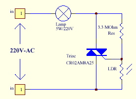
The series of light switches this time slightly different from the stress of work. The series of light switches can work directly on the AC power network. Light switches are using the main component of TRIAC and LDR. The circuit is very simple and the components were sold in the market. If you want a light reception sensitivity of this circuit can be arranged then the 3.3 MOhm resistor can be replaced with a variable resistor. For more details can be seen from the following series of images.

Triac  Light Switch circuit
Triac


Triac  Light Switch circuit series is priciple work as dimers, but dimers of control carried out by the reception of light around the LDR. The lower the intensity cayaha received LDR then semkin bright lights. For installation LDR need to be considered so as not exposed to light from the lamp directly.
Read More..

Friday, November 14, 2014

PHOTO SWITCH CIRCUIT USING NE 555

This is a simple photo switch suitable for home and industrial purpose. The circuit switches on a relay when the light intensity falling on the sensor crosses the set limit.The circuit is based on a NE 555 and two transistors for driving the relay. The resistor R1 is adjusted such a way that under normal condition the voltage across the LDR is less than 1/3 the supply voltage. In this condition output of IC is high .This makes transistor Q1 on. Transistor Q2′s base is connected to collector of Q1. So Q2 will be off keeping the relay de energized. When light falls the voltage across LDR rises above 2/3 Vcc. This makes the output of IC go high making the relay to energized. The result we get a relay that operates according to the intensity of light falling on the LDR.

Circuit Diagram and Parts List


Important Points

  • Assemble the circuit on a good quality PCB or common board.
  • To setup the circuit switch on power supply, connect a multimeter across LDR and adjust R1 so that voltage across LDR is just below 1/3 supply voltage. Ensure that relay is off in this condition. If not reduce voltage across LDR further more by adjusting R1 to make relay off.
  • Now cover the top of LDR using a black paper and see the relay gets activated. If not, make further adjustments with R1. Nothing to care after some trial and error you will get the correct set piont of R1 where the circuit works. This circuit  is nothing great, but some simple basics. I have tested this and got good results.
  • If there is some chattering in the relay, that may be because off the difference between the turning on and turning off voltages. This can be avoided by connecting a resistor whose value is equal to 1/2 the resistance of LDR at illuminated condition.
Read More..

Saturday, November 8, 2014

Battery Switch With Low Dropout Regulator

In the form of the LT1579 Linear Technology (www.linear-tech.com) has produced a practical battery switch with an integrated low-dropout regulator. In contrast to previous devices no diodes are required. The circuit is available in a 3.3 V version (LT1579CS8-3.3) and in a 5 V version (LT1579CS8-5), both in SO8 SMD packages. There is also an adjustable version and versions in an SO16 package which offer a greater range of control and drive signals. The main battery, whose terminal voltage must be at least 0.4 V higher than the desired output voltage, is connected to pin IN1. The backup battery is connected to pin IN2. The regulated output OUT can deliver a current of up to 300 mA. The LDO regulator part of the IC includes a pass transistor for the main input voltage IN1 and another for the backup battery on IN2.

Battery_Switch_With_LDO_Regulator_Circuit_Diagramw


The IC will switch over to the backup battery when it detects that the pass transistor for the main voltage input is in danger of no longer being able to maintain the required output voltage. The device then smoothly switches over to the backup battery. The open-drain status output BACKUP goes low to indicate when this has occurred. When neither battery is able to maintain the output voltage at the desired level the open-drain output DROPOUT goes low. The LT1579 can operate with input voltages of up to +20 V from the batteries. The regulator output OUT is short-circuit proof. The shutdown input switches off the output; if this feature is not required, the input can simply be left open.
Read More..

Sunday, November 2, 2014

RC Remote Control Switch

It is sometimes necessary for an RC (remote control) model to contain some kind of switching functionality. Some things that come to mind are lights on a model boat, or the folding away of the undercarriage of an aeroplane, etc. A standard solution employs a servo, which then actually operates the switch. Separate modules are also available, which may or may not contain a relay. A device with such functionality is eminently suitable for building yourself. The schematic shows that it can be easily realised with a few standard components.Picture of the project:
RC Switch Circuit

The servo signal, which consists of pulses from 1 to 2 ms duration, depending on the desired position, enters the circuit via pin 1 of connector K1. Two buffers from IC2 provide the necessary buffering after which the signal is differentiated by C2. This has the effect that at each rising edge a negative start signal is presented to pin 2 of IC1. D1 and R4 make sure that at the falling edge the voltage at pin 2 of IC2 does not become too high. IC1 (TLC555) is an old faithful in a CMOS version.

A standard version (such as the NE555) works just as well, but this IC draws an unnecessarily high current, while we strive to keep the current consumption as low as possible in the model. The aforementioned 555 is configured as a one-shot. The pulse-duration depends on the combination of R2/C1. Lowering the voltage on pin 5 also affects the time. This results in reducing the length of the pulse. In this circuit the pulse at the output of IC will last just over 1.5 ms when T1 does not conduct.Circuit diagram:
RC Switch Circuit Diagram

When T1 does conduct, the duration will be a little shorter than 1.5 ms. We will explain the purpose of this a little later on. Via IC2.C, the fixed-length pulse is, presented to the clock input of a D-flip-flop. As a consequence, the flip-flip will remember the state of the input (servo signal). The result is that when the servo-pulse is longer than the pulse form the 555, output Q will be high, otherwise the output will be low. It is possible, in practice, that the servo signal is nearly the same length as the output from the 555.

A small amount of variation in the servo signal could therefore easily cause the output to ‘chatter’, that is, the output could be high at one time and low the next. To prevent this chatter there is feedback in the form of R1, R3 and T1. This circuit makes sure that when the flip-flip has decided that the servo-pulse is longer than the 555’s pulse (and signals this by making output Q high), the pulse duration from the 555 is made a little shorter. The length of the servo-signal will now have to be reduced by a reasonable amount before the servo-pulse becomes shorter than the 555’s pulse.Parts and PCB layout:
Parts and PCB layout Of RC Switch

The moment this happens, T1 will stop conducting and the mono-stable time will become a little longer. The servo-pulse will now have to be longer by a reasonable amount before the flip-flip changes back again. This principle is called hysteresis. Jumper JP1 lets you choose between the normal or inverted output signals. Buffers IC2.D through to IC2.F together with R5 drive output transistor T2, which in turn drives the output. Note that the load may draw a maximum current of 100 mA. Diode D2 has been added so that inductive loads can be switched as well (for example, electrically operated pneu-matic valves).COMPONENTS LIST
Resistors:
R1 = 470k
R2 = 150k
R3 = 47k
R4 = 100k
R5 = 4k7
Capacitors:
C1 = 10nF
C2 = 1nF
C3,C4 = 100nF
Semiconductors:
D1 = BAT85 or similar Schottky diode
D2 = 1N4148
IC1 = CMOS 555 (e.g., TLC555 or ICM7555)
IC2 = 4049
IC3 = 4013
T1,T2 = BC547B
Miscellaneous:
JP1 = jumper with 3-way pinheader
K1 = servo cable
K2 = 2-way pinheader or 2 solder pins
Author: Paul Goossens - Copyright: Elektor Electronics
Read More..

Wednesday, September 24, 2014

Heat Sensitive Switch Circuit Diagram

Heat Sensitive Switch Circuit Diagram. At the heart of this heat-sensitive switch is IC LM35 (IC1), which is a linear temperature sensor and linear temperature-to-voltage converter circuit. The converter provides accurately linear and directly proportional output signal in millivolts over the temperature range of 0°C to 155°C. It develops an output voltage of 10 mV per degree centigrade change in the ambient temperature. Therefore the output voltage varies from 0mV at 0°C to 1V at 100°C and any voltage measurement circuit connected across the output pins can read the temperature directly. The input and ground pins of this heat-to-voltage converter IC are connected across the regulated power supply rails and decoupled by R1 and C1. Its temperature-tracking output is applied to the non-inverting input (pin 3) of the comparator built around IC2. The inverting input (pin 2) of IC2 is connected across the positive supply rails via a voltage divider network formed by potentiometer VR1. Since the wiper of potentiometer VR1 is connected to the inverting input of IC2, the voltage presented to this pin is linearly variable. 

Circuit diagram :
Heat Sensitive Switch  Circuit Diagram Heat Sensitive Switch  Circuit Diagram

This voltage is used as the reference level for the comparator against the output supplied by IC1. So if the non-inverting input of IC2 receives a voltage lower than the set level, its output goes low (approximately 650 mV). This low level is applied to the input of the load-relay driver comprising npn transistors T1 and T2. The low level presented at the base of transistor T1 keeps it nonconductive. Since T2 receives the forward bias voltage via the emitter of T1, it is also kept non-conductive. Hence, relay RL1 is in de-energised state, keeping mains supply to the load ‘off’ as long as the temperature at the sensor is low. Conversely, if the non-inverting input receives a voltage higher than the set level, its output goes high (approximately 2200mV) and the load is turned ‘on.’ This happens when IC1 is at a higher temperature and its output voltage is also higher than the set level at the inverting input of IC2. So the load is turned on as soon as the ambient temperature rises above the set level. 

Capacitor C3 at this pin helps iron out any ripple that passes through the positive supply rail to avoid errors in the circuit operation. By adjusting potentiometer VR1 and thereby varying the reference voltage level at the inverting input pin of IC1, the temperature threshold at which energisation of the relay is required can be set. As this setting is linear, the knob of potentiometer VR1 can be provided with a linear dial calibrated in degrees centigrade. Therefore any temperature level can be selected and constantly monitored for external actions like turning on a room heater in winter or a room cooler in summer. The circuit can also be used to activate emergency fire extinguishers, if positioned at the probable fire accident site. The circuit can be modified to operate any electrical appliance. In that case, relay RL1 must be a heavy-duty type with appropriately rated contacts to match the power demands of the load to be operated.


Author : M.K. Chandra Mouleeswaran & Miss Kalan Priya - Copyright :  EFY
Read More..

Heat Sensitive Switch Circuit Diagram

Heat Sensitive Switch Circuit Diagram. At the heart of this heat-sensitive switch is IC LM35 (IC1), which is a linear temperature sensor and linear temperature-to-voltage converter circuit. The converter provides accurately linear and directly proportional output signal in millivolts over the temperature range of 0°C to 155°C. It develops an output voltage of 10 mV per degree centigrade change in the ambient temperature. Therefore the output voltage varies from 0mV at 0°C to 1V at 100°C and any voltage measurement circuit connected across the output pins can read the temperature directly. The input and ground pins of this heat-to-voltage converter IC are connected across the regulated power supply rails and decoupled by R1 and C1. Its temperature-tracking output is applied to the non-inverting input (pin 3) of the comparator built around IC2. The inverting input (pin 2) of IC2 is connected across the positive supply rails via a voltage divider network formed by potentiometer VR1. Since the wiper of potentiometer VR1 is connected to the inverting input of IC2, the voltage presented to this pin is linearly variable. 

Circuit diagram :
Heat Sensitive Switch  Circuit Diagram Heat Sensitive Switch  Circuit Diagram

This voltage is used as the reference level for the comparator against the output supplied by IC1. So if the non-inverting input of IC2 receives a voltage lower than the set level, its output goes low (approximately 650 mV). This low level is applied to the input of the load-relay driver comprising npn transistors T1 and T2. The low level presented at the base of transistor T1 keeps it nonconductive. Since T2 receives the forward bias voltage via the emitter of T1, it is also kept non-conductive. Hence, relay RL1 is in de-energised state, keeping mains supply to the load ‘off’ as long as the temperature at the sensor is low. Conversely, if the non-inverting input receives a voltage higher than the set level, its output goes high (approximately 2200mV) and the load is turned ‘on.’ This happens when IC1 is at a higher temperature and its output voltage is also higher than the set level at the inverting input of IC2. So the load is turned on as soon as the ambient temperature rises above the set level. 

Capacitor C3 at this pin helps iron out any ripple that passes through the positive supply rail to avoid errors in the circuit operation. By adjusting potentiometer VR1 and thereby varying the reference voltage level at the inverting input pin of IC1, the temperature threshold at which energisation of the relay is required can be set. As this setting is linear, the knob of potentiometer VR1 can be provided with a linear dial calibrated in degrees centigrade. Therefore any temperature level can be selected and constantly monitored for external actions like turning on a room heater in winter or a room cooler in summer. The circuit can also be used to activate emergency fire extinguishers, if positioned at the probable fire accident site. The circuit can be modified to operate any electrical appliance. In that case, relay RL1 must be a heavy-duty type with appropriately rated contacts to match the power demands of the load to be operated.


Author : M.K. Chandra Mouleeswaran & Miss Kalan Priya - Copyright :  EFY
Read More..

Simple Sound Activated Switch

Simple Sound Activated Switch Circuit diagram : Control by sound may be very useful,  not just on a robot but also for a bit  of home automation, for example a  sound activated light responding to a  knock on the door or a hand clap. The  light will be automatically switched  off after a few seconds. An alternative  use is burglar protection — if someone  wants to open the door or break some-thing the light will come on, suggesting  that someone’s at home. The circuit can work from any 5– 12 VDC regulated power supply pro-vided a relay with the suitable coil voltage is used.
 
Simple Sound Activated Switch Circuit diagram :


Sound Activated Switch Circuit Diagram

When you first connect the supply  voltage to the circuit, the relay will  be energised because of the effect of capacitor C2. Allow a few seconds for  the relay to be switched off. You can  increase or decrease the ‘on’ period  by changing the value of C2. A higher  value results in a longer ‘on’ period,  and vice versa. Do not use a value  greater than 47 µF. Biasing resistor R1 determines to a  large extent the microphone sensitivity. An electret microphone usually has  one internal FET inside which requires  a bias voltage to operate. The optimum  bias level for response to sound has to  be found by trial and error.
 
All relevant electrical safety precautions should be observed when connecting mains powered loads to the relay contacts.
Read More..

Video Switch for Intercom System

Video Switch for Intercom System Circuit Diagram. Nowadays a lot of intercom units are  equipped with video cameras so that you can  see as well as hear who is at the door. Unfortunately, the camera lens is perfectly placed  to serve as a sort of support point for people  during the conversation, with the result that  there’s hardly anything left see in the video  imagery.  One way to solve this problem is to install two cameras on the street side instead only  one, preferably some distance apart. If you  display the imagery from the two cameras  alternately, then at least half of the time you  will be able to see what is happening in front  of the door. Thanks to the video switch module described  here, which should be installed on the street  side not too far away from the two cameras,  you need only one monitor inside the house and you don’t need to install any additional video cables.
 
Circuit diagram :
Video Switch for Intercom System-Circuit-Diagram
Video Switch for Intercom System Circuit Diagram

Along with a video switch, the circuit includes  a video amplifier that has been used with  good results in many other Elektor projects,  which allows the brightness and the contrast  to be adjusted separately. This amplifier is  included because the distance between the  street and the house may be rather large, so it is helpful to be able to compensate for cable attenuation in this manner.  The switch stage is built around the well  known 4060 IC, in which switches IC2a and  IC2d alternately pass one of the two signals to  the output. They are driven by switches IC2b and IC2c, which generate control signals that  are 180 degrees out of phase. The switching rate for the video signals is  determined by a clock signal from an ‘old  standby’ 555 IC, which causes the signals to  swap every 2 seconds with the specified com ponent values.
 
Naturally, this circuit can also used in many other situations, such as where two cameras are needed for surveillance but only one video cable is available.
Read More..

Wednesday, September 3, 2014

Simple ON OFF Touch Switch with 555 Schematic

This simple ON OFF touch switch schema is based on the well known timer IC 555 (IC1), which drives a relay that acts like a switch. The metal surfaces can have what form we want, but it should be clean and very close to the schema.

Read more  WC fan using 555

Touch plate MP1 in order to close the contact of relay RL1 [ON], or plate MP2 in order to open the contact of RL1 [OFF]. The Led D2 turns on when the contacts of RL1 are closed. Two small pieces of metal can be used as sensor plates.

555 ON/OFF Touch Switch Schematic

Simple

Parts List
R1 = R2 = 3.3M
R3 = 10K
R4 = 1K
C1 = 10nF
D1 = 1N4007
Q1 = BC547
IC = NE555
12V relay
Read More..

Friday, April 12, 2013

Clap Switch Circuit Diagram

Here’s a clap switch free from false triggering. To turn on/off any appliance, you just have to clap twice. The circuit changes its output state only when you clap twice within the set time period. Here, you’ve to clap within 3 seconds. 

The clap sound sensed by condenser microphone is amplified by transistor T1. The amplified signal provides negative pulse to pin 2 of IC1 and IC2, triggering both the ICs. IC1, commonly used as a timer, is wired here as a monostable multivibrator. Trigging of IC1 causes pin 3 to go high and it remains high for a certain time period depending on the selected values of R7 and C3. 

This ‘on’ time (T) of IC1 can be calculated using the following relationship: T=1.1R7.C3 seconds where R7 is in ohms and C3 in microfarads. On first clap, output pin 3 of IC1 goes high and remains in this standby position for the preset time.Also, LED1 glows for this period. The output of IC1 provides supply voltage to IC2 at its pins 8 and 4.
Circuit diagram :
Clap Switch  Circuit Diagram
Clap Switch Circuit Diagram

Now IC2 is ready to receive the triggering signal. Resistor R10 and capacitor C7 connected to pin 4 of IC2 prevent false triggering when IC1 provides the supply voltage to IC2 at first clap. On second clap, a negative pulse triggers IC2 and its output pin 3 goes high for a time period depending on R9 and C5.

 This provides a positive pulse at clock pin 14 of decade counter IC 4017 (IC3). Decade counter IC3 is wired here as a bistable. Each pulse applied at clock pin 14 changes the output state at pin 2 (Q1) of IC3 because Q2 is connected to reset pin 15. The high output at pin 2 drives transistor T2 and also energizes relay RL1. LED2 indicates activation of relay RL1 and on/off status of the appliance. A free-wheeling diode (D1) prevents damage of T2 when relay de-energizes.
 
 
http://streampowers.blogspot.com/2012/06/clap-switch-circuit-diagram.html
Read More..

Saturday, April 6, 2013

5 VOLT MOMENTARY OPERATION TOUCH SWITCH

This simple circuit uses a single IC to form a nice touch switch circuit.  A single transistor forms the remote active switch sensor.  Multiple switches can be wired in parallel.  The switch circuit can be located about 500 feet from the control circuit.
s
Read More..