Showing posts with label simple. Show all posts

Saturday, November 8, 2014

Simple Pulse train to sinusoid converter

The circuit letsyou convert a serial pulse stream or sinusoidal input to a sinusoidal output at 1/32 the frequency. By varying the frequency of Vrn, you can achieve an output range ofl07:1-from about 100 kH2 to less than 0.01 H2. The output resembles that of a 5-bit d/a converter operating on paralleLdigital data. Counter IC1 generates binary codes that repeatedly scan the range from 00000 to 11111. The output amplifier adds the corresponding XOR gate outputs, Vvv or ground, weighted by the values of input resistors R1 through R4.


The 16 counter codes 00000 to 01111, for instance, pass unchanged to the XOR gate outputs, and cause Vom to step through the half-sinusoidal cycle for maximum amplitude to minimum amplitude. Counter output Q4 becomes high for the next 16 codes, causing the XOR gates to invert the QO through Q3 outputs. As a result, VouT steps through the remaining half cycle from minimum to maximum amplitude. The counter then rolls over and initiates the next cycle. You can change the R1 through R4 values to obtain other VouT waveforms. VDv should be at least 12 V to assure maximum-frequency operation from IC1 to IC2.
Read More..

Monday, November 3, 2014

A Small and Simple Bench Amplifier

A small 325mW amplifier with a voltage gain of 200 that can be used as a bench amplifier, signal tracer or used to amplify the output from personal radios, etc. The circuit is based on the National Semiconductor LM386 amplifier. In the diagram above, the LM386 forms a complete non-inverting amplifier with voltage gain of x200. A datasheet in PDF format can be downloaded from the National Semiconductor website. The IC is available in an 8 pin DIL package and several versions are available; the LM386N-1 which has 325mW output into an 8 ohm load, the Lm386N-3 which has 700mW output and the LM386N-4 which offers 1000mW output.

 all versions work in this circuit. The gain of the Lm386 can be controlled by the capacitor across pins 1 and 8. With the 10u cap shown above, voltage gain is 200, omitting this capacitor and the gain of the amplifier is 20.

Very Simple Bench Amplifier Finished Project

Bench

Bench Amplifier Circuit Diagram

Bench

The IC works from 4 to 12Volts DC, 12Volt being the maximum recommended value. The internal input impedance of the amplifier is 50K, this is shunted with a 22k log potentiometer so input impedance in this circuit will be lower at about 15k. The input is DC coupled so care must be taken not to amplify any DC from the preceeding circuit, otherwise the loudspeaker may be damaged. A coupling capacitor may included in series with the 22k control to prevent this from happening.


Read More..

Wednesday, September 24, 2014

Simple Electronic Door Lock Circuit Diagram

Its easy to build and straight forward. This electronic door lock has a remarkable conception because it uses only one active component. How does it work?

Electronic Door Lock Circuit Diagram


Simple Electronic Door Lock  Circuit Diagram

To put the relay in tension the 4 buttons S1 – S4 must be pressed. If anyone of the 4 butoons S5 – S8 are pushed the relay doesn’t switch. The supply voltage must be equal to the working voltage of the relay. One transistor like BD135 can switch up to 0.5A, at the same time 2N2222 can do only 0.2A.
Read More..

Simple CD Player Adapter For Car

Whenever Im in the car listening to my favourite CD, it always happens; my batteries go dead. To solve that problem, I built this extremely simple regulator circuit. It steps down the 12V from the lighter socket to 9V which is used by the CD player. Different CD players (I have a Sony Discman) may require different voltages, so just use the correct regulator. All the 78xx series regulators have the same pin out, so the circuit is universal.


Part           Total Qty.                     Description

C1                      1                        1000uF 25V Electrolytic Capacitor   
C2                      1                        10uF 25V Electrolytic Capacitor   
C3                      1                        1uF 15V Elextrolytic Capacitor   
C4                      1                        0.1uF 15V Electrolytic Capacitor   
U1                      1                        7809 Or Other Regulator (See "Notes")    See Notes
MISC                  1                        Cigarette Lighter Plug, Plug For CD Player (See "Notes"),      Heat Sink For U1, Wire, Case.   
   
Notes
  • The voltage your CD player needs will determine which regulator you use. For 9V, use the 7809. For 6V, use the 7806. For the unlikely 5V use the 7805. Remember that whatever regulator you use, you will need to heat sink it. The metal case or metal cover on the case makes a great heat sink.
  • I built the circuit in a small case with the long wire to the cigarette lighter plug coming out one end, then another, slightly shorter wire going out the other end to the CD player.
  • Triple check your wiring. You would hate to ruin an expensive CD player because you reversed one of the connections or hooked the regulator up backwards. Link
Read More..

Simple Battery Charger Vehicle Circuit Diagram

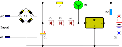
Unlike many boots, this battery charger continuously charges the maximum current, decreasing only near full battery voltage. In this case the full load current source, transformer / rectifier was 4.4A. It tapers to 4A 13.5V, 14.0V 3A, 2A 14.5V and 15.0V in 0A.


Simple Battery Charger Vehicle Circuit Diagram

Simple Battery Charger Vehicle Circuit Diagram


Parts:

Resistors
R1 = 0.32R
R2 = 8.2R Capacitors
C1 = x 10,000 uF 63V
D1 = 1N4004
D2 = 1N4004
D3 = 1N4004
Q1 = MJ1504
IC REG = 7815
BR1 = 1N4004x4
B1 = 12 Volt Battery
TR 20 volts AC

R1 and R2 are as high power resistor 2W, 3W, 5W or higher. Q1 and IC requires a heatsink good. If they are mounted on the same heatsink and will decrease the circuit turns Q1 gets too hot.
Read More..

Simple 1KHz Sine wave Generator Circuits Diagram

This simple circuit generates a good 1KHz sine wave adopting the inverted Wain bridge configuration (C1-R3 & C2-R4). It features a variable output, low distortion and low output impedance in order to obtain good overload capability. A small filament bulb ensures a stable long term output amplitude waveform. 

1KHz Sine wave Generator Circuits Diagram

 Notes:
  • The bulb must be a low current type (12V 40-50mA or 6V 50mA) in order to obtain good long term stability and low distortion.
  • Distortion @ 1V RMS output is 0.15% using a 12V 40mA bulb, raising to 0.5% with a 12V 100mA one.
  • Using a bulb differing from specifications may require a change of R6 value to 220 or 150 Ohms to ensure proper circuits oscillation.
  • Set R5 to read 1V RMS on an Audio Millivoltmeter connected to the output with R7 rotated fully clockwise, or to view a sinewave of 2.828V Peak-to-Peak amplitude on the oscilloscope.
  • With C1, C2 = 100nF the frequency generated is 100Hz and with C1, C2 = 1nF frequency is 10KHz but R5 requires adjustment.
  • High gain transistors are preferred for better performance.

Parts:

R1____________5K6  1/4W Resistor
R2____________1K8  1/4W Resistor
R3,R4________15K   1/4W Resistors
R5__________500R   1/2W Trimmer Cermet
R6__________330R   1/4W Resistor
R7__________470R   Linear Potentiometer
 
C1,C2________10nF  63V Polyester Capacitors
C3__________100µF  25V Electrolytic Capacitor
C4__________470nF  63V Polyester Capacitor
 
Q1,Q2_______BC238  25V 100mA NPN Transistors
 
LP1___________12V  40mA Filament Lamp Bulb (See Notes)
 
J1__________Phono chassis Socket
 
SW1__________SPST  Slider Switch
 
B1_____________9V  PP3
 
Clip for 9V PP3 Battery

Read More..

Simple 12V to 250V Converter

A very simple portable 12v to 250V converter can be designed using this circuit diagram. This 12 to 250V converter is designed for portable use with a 12 V car battery.A built astabil multivibrator T1 and T2 generates a rectangular wave at a frequency of 50 Hz. As T1 and T2 drive alternative exit stage system also works in "push-pull". When T1 lead by passing a current T3: T5 and that it engages the latter transistor connects to a half battery of 12 V secondary winding of the transformer Tr When T2 network drive, T6 transistor coupled to the battery the other half of the network adapter.


 If it is used for output stages 40 411 RCA transistors, the current through secondary winding can be up to 10 A, giving a power output of 180 watts. If you use 2N3055 transistors, power output will be about 90 watts. Since the output transistors are driven to saturation, they have very high mounted radiators.Although circuit is simple construction and has high efficiency disadvantage is rectangular output voltage which, in the absence of a regulator is dependent on task: small loads, the output voltage is 250 V ac (not working properly for the engine speed control, light dimmers, televisions, hi-fi equipment.
Read More..

A Simple Hybrid Audio Amplifier Circuit

A Simple Hybrid Audio Amplifier Circuit diagram. The debate still goes on as to which are better, valves or transistors. We don’t intend to get involved in that argument here. But if you can’t make your mind up, you should try out this simple amplifier. This amplifier uses a valve as a pre-amplifier and a MOSFET in the output stage. The strong negative feedback makes the frequency response as flat as a pancake. In the prototype of the amplifier we’ve also tried a few alternative components. For example, the BUZ11 can be replaced by an IRFZ34N and an ECC83 can be used instead of the ECC88. In that case the anode voltage should be reduced slightly to 155 V. The ECC83 (or its US equivalent the 12AX7) requires 2 x 6.3 V for the filament supply and there is no screen between the two triodes, normally connected to pin 9. This pin is now connected to the common of the two filaments.

Project Image :
A simple-hybrid-amp-circuit

The filaments are connected to ground via R5. If you’re keeping an eye on the quality, you should at least use MKT types for coupling capacitors C1, C4 and C7. Better still are MKP capacitors. For C8 you should have a look at Panasonic’s range of audio grade electrolytics. P1 is used to set the amount of negative feedback. The larger the negative feedback is, the flatter the frequency response will be, but the smaller the overall gain becomes.
Circuit diagram:
simple-hybrid-amp-circuit-diagram
Simple Hybrid Audio Amplifier Circuit Diagram

With P2 you can set the quiescent current through T2. We have chosen a fairly high current of 1.3 A, making the output stage work in Class A mode. This does generate a relatively large amount of heat, so you should use a large heatsink for T2 with a thermal coefficient of 1 K/W or better. For L1 we connected two secondary windings in series from a 2x18V/225 VA toroidal transformer. The resulting inductance of 150 mH was quite a bit more than the recommended 50 mH. However, with an output power of 1 W the amplifier had difficulty reproducing signals below 160 Hz. The distortion rose to as much as 9% for a signal of 20 Hz at 100 mW. To properly reproduce low-frequency signals the amplifier needs a much larger coil with an iron core and an air gap. This prevents the core from saturating when a large DC current flows through the coil.

Parts layout:
Parts layout

Such a core may be found in obsolete equipment, such as old video recorders. A suitable core consists of welded E and I sections. These transformers can be converted to the required inductor as follows: cut through the welding, remove the windings, add 250 to 300 windings of 0.8 mm enamelled copper wire, firmly fix the E and I sections back together with a piece of paper in between as isolation. The concepts used in this circuit lend themselves very well to some experimentation. 

The number of supply voltages can be a bit of a problem to start with. For this reason we have designed a power supply especially for use with this amplifier (Quad power supply for hybrid amp). This can of course just as easily be used with other amplifiers. The supply uses a cascade stage to output an unstabilised voltage of 170 V for the SRPP (single rail push pull) stage (V1).


PCB layout:
PCB layout

During initial measurements we found that the ripple on this supply was responsible for a severe hum at the output of the amplifier. To get round this problem we designed a separate voltage regulator (High-voltage regulator with short circuit protection), which can cope with these high voltages. If you use a separate transformer for the filament supply you can try and see if the circuit works without R5. During the testing we used a DC voltage for the filament supply. 

Although you may not suspect it from the test measurements (see table), this amplifier doesn’t sound bad. In fact, it is easily better than many consumer amplifiers. The output power is fairly limited, but is still enough to let your neighbours enjoy the music as well. It is possible to make the amplifier more powerful, in which case we recommend that you use more than one MOSFET in the output stage. The inductor also needs to be made beefier. Since this is a Class A amplifier, the supply needs to be able to output the required current, which becomes much greater at higher output powers. The efficiency of the amplifier is a bit over 30%.


Author: Frans Janssens - Copyright: Elektor Electronics
Read More..

A Simple Yet Useful Video Switcher

With the cost of security cameras going down, adding a surveillance system for your store, office or home is becoming more practical all the time. However, you might be dismayed at the thought of having to buy a monitor for every camera that’s installed. dedicating a single monitor to a single camera also runs the risk of burning the camera’s image into the phosphor screen of the CRT. If you prefer a single monitor instead of the “NASA-Mission Control” look, you could buy a special monitor that has a video switcher built in. That type of monitor can automatically switch between several camera inputs in sequence.

 Useful Video Switcher Circuit Diagram

Useful Video Switcher


With that type of arrangement, you’d have to watch only one screen instead of having to scan a wall of CRTs. Switching between several cameras would also prevent image burn-in on the monitor. Those types of monitors, unfortunately, are also very expensive, offsetting the cost savings of even the cheapest surveillance camera. Video switchers are also available, but the cost of a switcher and a monitor could be as expensive as a monitor/switcher combination unit. A viable alternative for a video switcher is to build your own. Thanks to some recently introduced ICs, the cost and effort of designing and building such a unit has become both quite affordable and easy.


The video switcher described here can display the output of two, three, or four cameras on a single monitor. The number of cameras is set by a DIP switch on the circuit board. That feature avoids blank displays if less than four cameras are used by sequencing through only the inputs that are connected to a camera. In the automatic mode, the cameras are switched at a rate that can be varied with a panel mounted control. The switching rate can be set from about once per second to about once every 20 seconds. In the manual mode, one camera output is displayed continuously. A momentary-toggle switch is then used to step through the various cameras.

How it works

The heart of the video switcher is a Maxim MAX454. That integrated circuit contains a four-way video multiplexer and an amplifier that operates as a low-impedance line driver. The resulting video output is high quality with very low phase distortion. The video inputs are selected by applying a binary number to the address inputs. The binary number is also used to light a series of LEDs that indicate whichh camera input is currently selected. The circuit is powered by a 9-volt AC wall-adapter transformer, two diodes, and two voltage regulators.

Circuit description

Figure 1 is a schematic diagram of the video switcher. Multiplexer IC1 has four video inputs, two address inputs, one video output, one external amplifier input, and and three power terminals. The video cameras connect to the video inputs through J1-J4. The inputs are terminated with 75 ohm resistors R1-R4. The gain of the internal video amplifier is set by a feedback network connected to pin 13 of IC1. That feedback network consists of R5-R8 and C3. The gain is set to 2 in order to compensate for any loss through the 75 ohm terminator resistor, R9. The resulting net gain is 1 at output J5.

The binary addressing circuit is built around IC2, a CD4017 decade counter. That chip produces one positive output at a time on each of its ten outputs in sequence for every clock pulse. The first four outputs at pins 3,2,4,and 7 are connected to transistors Q1- Q4. Those transistors drive LED1-LED4 through current limiting resistor R15. The outputs from IC2 (pins 2,4, and 7) are also decoded into binary logic by diodes D1-D4. The binary logic is sent to the address input lines of IC1.


The number of cameras connected to the video switcher is set with S1. Each switch in S1 is connected to an output from IC2. If, for example, there are only two cameras connected to the video switcher, S1-a is closed. That connects the third output to IC2’s reset line. When IC2 advances to the third count, that output passes through S1-a to the reset, and IC2 resets to zero, activating the first camera. The sequence would be camera 1, camera 2, then back to camera 1. Closing S1-b or S1-c instead of S1-a will let the video switcher cycle through three or four cameras, respectively.

Clock pulses for the counter are generated by IC3, an LMC555 CMOS timer. The pulse rate and pulse width is controlled by C4, R10, R11 and potentiometer R12. By adjusting R12, the output frequency of IC3 can be controlled between 1 Hz and 1/20 Hz. The clock pulses from IC3 are connected to IC2 through S2, a three position toggle switch. Switching S2 to the auto position lets the pulses from IC3 select the next camera at a rate set by R12. When S2 is in its center-off position, no switching takes place, and whatever camera input is selected is passed through to the output.


The select position on S2 is a momentary contact. That position raises the clock input of IC2 to 5 volts, which increments the binary count and selects the next camera. When S2 is released, it springs back to its center-off position. The clock input of IC2 is then held at a low-logic level by R13. The MAX454 requires ±5 volts while the other ICs require only +5 volts. Power is supplied by AC adapter T1, rectifier diodes D5 and D6, regulators IC4 and IC5, and filter capacitors C6-C9.

Construction

Because of the high frequency video signals involved, the video switcher should be built on a printed circuit board. The circuit is simple enough to fit onto a single-sided board with only two jumpers needed. A foil pattern is included for etching and drilling your own board. Alternatively, an etched board can be purchased from the source given in the parts list. A feature of that board design is ground traces that run between all of the video signal traces in order to keep induced noise and crosstalk between the signals to a minimum.

Weather you etch a board from the foil pattern or purchase one from the source in the parts list, use the parts-placement diagram in fig. 2 for component placement. It is easiest to install and solder the resistors and diodes first. Once those components are in place, scrap component leads can be used for the two jumper wires. Next, install S1 and sockets for IC2 and IC3. Do not use a socket for IC1, the MAX454 multiplexer.

When installing J1-J5, hold the connectors tight against the board while soldering the center pin. The assembly can then be placed on a heat-resistant surface and the ground pins soldered. Because of their size and mass, a larger soldering iron might be needed to solder J1-J5. Otherwise the board might be damaged if heat is applied too long. Once the connectors are soldered in place, Q1-Q4, IC4, IC5, and all the capacitors can be installed. The LEDs should be installed next, leaving their leads long so that they can be bent to reach through the front panel of the enclosure.

Double-check the orientation of the polarized components, so that they are not installed backwards by accident. Once a component is soldered in place, removing it becomes much more difficult. Solder two 3-inch long wires onto the two terminals of R12 that are clockwise when viewing the potentiometer from the back. Connect those wires to the holes for R12 on the board. Three additional 3-inch long wires are soldered onto the terminals of S2. The center terminal connects to the hole near C5 and R13.

The momentary-contact terminal connects to the hole near R14. The remaining terminal connects to the hole near IC3 and R10. Solder IC1 directly onto the circuit board. That will result in the shortest possible lead length for the video signals. Plug IC2 and IC3 into their sockets, being careful to handle them as static-sensitive CMOS devices. Solder the T1 leads onto the board. Examine the board for any wiring errors, bad solder joints, and incorrect components. Once the assembly is inspected, it can be tested.

Testing

Plug T1 into an AC outlet and measure the voltages across C8 nd C9. The voltage across C8 should measure +5 volts. Across C9, the voltage should be -5 volts. To select two cameras, set S1-a on; to select three cameras, set set S1-b on; and to select all four cameras, set S1-c on. Only one switch at a time should be on. When switch S2 is toggled to its momentary position, the LEDs should sequence to the next indicator each time S2 is toggled. The order of the LEDs should cycle from 1 through 4 and repeat. When S2 is set to automatic, the LEDs should automatically at a rate that should vary as potentiometer R12 is adjusted. Connect cameras to J1-J4 and a monitor to J5.

The video signal on the monitor should switch from camera to camera according to the LEDs. After testing is completed, drill appropriate holes in a suitable enclosure for J1-J5, LED1-LED4, S2, and R12. Mount the board in the enclosure using the mounting hardware for J1-J5 to hold it in place. Mount R12 and S2 in the front panel and bend the LEDs so they fit through the holes in the panel. The hole for the T1 wire should be drilled at a point where the two halves of the enclosure meet.

Tie a knot in the wire for strain relief and place the wire in the enclosure hole with the knot on the inside of the enclosure before closing the case. That completes the project. If all has gone well, as is likely, your video switcher is now ready for use.

SEMICONDUCTORS
  • IC1 - MAX454 multiplexer, integrated circuit (MAXIM)
  • IC2 - CD4017 decade counter, integrated circuit
  • IC3 - LMC555 timer, integrated circuit
  • IC4 - 78l05 voltage regulator, integrated circuit
  • IC5 - 79l05 voltage regulator, integrated circuit
  • Q1-Q4 - MPSA14, NPN transistor
  • D1-D4 - 1N914, silicon diode
  • D5, D6 - 1N4004, silicon diode
  • LED1-LED4 - Light emitting diode, red
RESISTORS
  • R1-R4, R9-R15 - 75 ohm
  • R5 - 150,000 ohm
  • R6 - 620 ohm
  • R7 - 1100 ohm
  • R8 - 1000 ohm
  • R10 - 10,000 ohm
  • R11 - 51,000 ohm
  • R12 - I megohm potentiometer, panel mount
  • R13, R14 - 100,000 ohm
CAPACITORS
  • C1,C2,C5 - 0.1mF, 50WVDC, metalized film
  • C3 - 6.8 pF, ceramic disc
  • C4 - 10 mF, 50 WVDC, low leakage electrolytic
  • C5, C7 - 470 mF, 25 WVDC, electrolytic
  • C8, C9 - 100 mF, 16 WVDC, electrolytic
ADDITIONAL PARTS AND MATERIALS
  • S1 - DIP switch, 3 position
  • S2 - Toggle switch, single pole double throw, one momentary position
  • J1-J5 - Video connector, chassis mount, “F” type
  • T1 - 9 volt AC wall adapter transformer, PC board, IC sockets, LED holders, 22 gauge hookup wire, knob, enclosure, hardware, etc.
Read More..

Simple Horn Bugle Electronic Circuit Diagram

This Simple Horn Bugle Electronic Circuit Diagram just a door trigger input 4093, bound in a low frequency oscillator, as the transistor Q1, which is the IRF511 FET amplifier is directly connected to a small speaker with horn. The output frequency can be changed by adjusting potentiometer R1.


Simple Horn Bugle Electronic Circuit Diagram

Simple Horn Bugle Electronic Circuit Diagram

Read More..

Simple Sound Activated Switch

Simple Sound Activated Switch Circuit diagram : Control by sound may be very useful,  not just on a robot but also for a bit  of home automation, for example a  sound activated light responding to a  knock on the door or a hand clap. The  light will be automatically switched  off after a few seconds. An alternative  use is burglar protection — if someone  wants to open the door or break some-thing the light will come on, suggesting  that someone’s at home. The circuit can work from any 5– 12 VDC regulated power supply pro-vided a relay with the suitable coil voltage is used.
 
Simple Sound Activated Switch Circuit diagram :


Sound Activated Switch Circuit Diagram

When you first connect the supply  voltage to the circuit, the relay will  be energised because of the effect of capacitor C2. Allow a few seconds for  the relay to be switched off. You can  increase or decrease the ‘on’ period  by changing the value of C2. A higher  value results in a longer ‘on’ period,  and vice versa. Do not use a value  greater than 47 µF. Biasing resistor R1 determines to a  large extent the microphone sensitivity. An electret microphone usually has  one internal FET inside which requires  a bias voltage to operate. The optimum  bias level for response to sound has to  be found by trial and error.
 
All relevant electrical safety precautions should be observed when connecting mains powered loads to the relay contacts.
Read More..

Simple Subwoofer Lowpass Filter using uA741 Single Op Amp Ic

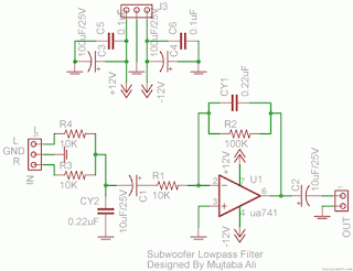
This is the simplest Sub woofer Low Pass filter Circuit using uA741 single op amp ic. The circuit is very low cost with respect to their work. The cut off frequency of this circuit is 25Hz to 80Hz maximum. Using this circuit , you can easily design a 2.1 Sub-woofer Speaker System at your own Home. The circuit contains very few components.In Pakistan, the cost of this circuit with PCB is Rs:45 The same circuit is working in my own hand made sub-woofer system. So Try this [Link]

Lowpass Filter using uA741 Single Op-Amp Ic
Parts List: 

R1,R3,R4 = 10K 1/4W
R2=100K 1/4W
CY1,CY2 = 0.22uF Polyester
C1,C2 = 10uF/25V Electrolytic
IC1 = uA741A Single Op-Amp Ic + 8 Pin Ic Socket
3 Pin Male & Female Connector x 2
2 Pin Male & Female Connector x 1
PCB as in required size 4.5 cm x 3.4 cm
Read More..

Saturday, September 13, 2014

Simple Pulse Oximeter Wiring diagram Schematic


This schema is a pulse oximeter, it is a medical device to indirectly measure the amount of oxygen in the blood of a person. The schema is very simple and inexpensive to build, the sensor to be monitored only need an oscilloscope, but the case does not have an oscilloscope, here an article on how to make your pc a Oscilloscope. The operation is simple, light from an LED shines through on one side of your finger and is measured across the photo-transistor, a clothespin wood will engage the LED and the photo-transistor as a way to mount and align the sensor with finger.

The monitor schema uses only a single IC LM324 operational amplifier. There are three basic steps, the input signal is decoupled before being pre-amplified then passes through an adjustable low-pass filter to help eliminate noise 60Hz AC and finally a further low-pass filter in parallel with amplifier.

Pulse Oximeter Circuit Diagram

Simple

Read More..

Wednesday, September 3, 2014

Simple ON OFF Touch Switch with 555 Schematic

This simple ON OFF touch switch schema is based on the well known timer IC 555 (IC1), which drives a relay that acts like a switch. The metal surfaces can have what form we want, but it should be clean and very close to the schema.

Read more  WC fan using 555

Touch plate MP1 in order to close the contact of relay RL1 [ON], or plate MP2 in order to open the contact of RL1 [OFF]. The Led D2 turns on when the contacts of RL1 are closed. Two small pieces of metal can be used as sensor plates.

555 ON/OFF Touch Switch Schematic

Simple

Parts List
R1 = R2 = 3.3M
R3 = 10K
R4 = 1K
C1 = 10nF
D1 = 1N4007
Q1 = BC547
IC = NE555
12V relay
Read More..

Sunday, May 26, 2013

Simple door Alarm circuit

This is simple door alarm circuit.You can attach this circuit for your for your main door If somebody opens it alarm will activate.Sw1 is a Read switch.Those switches are operated with magnets.
Parts:

Q1 = BC547
Q2 = BC327
B1 = 3V Battery
R1 = 330K
R2 = 100R
C1 = 10nF-63V
C2 = 100uF-25V
SW1 = Read Switch


Note

# Dont supply more than 4.5V for this circuit

#Attach a magnet for the door frame near by the read switch
Read More..

Wednesday, April 10, 2013

Simple Voltmeter Circuit

his circuit provides a simple means to determine the voltage of a low-impedance voltage source. It works as follows. P1, which is a 1-W potentiometer, forms a voltage divider in combination with R1. The voltage at their junction is buffered by T1, and then passed to reference diode D1 via R3. D1 limits the voltage following the resistor to 2.5 V. An indicator stage consisting of T2, R4 and LED D2 is connected in parallel with D1. As long as the voltage is not limited by D1, the LED will not be fully illuminated. This is the basic operating principle of this measurement circuit.
 
Simple Voltmeter Circuit Diagram1
Read More..

Friday, April 5, 2013

Mini and simple power amplifier

low power amplifier

What is the meaning of the picture above? The above picture is a miniature audio amplifier and very simple. Here I will give an audio amplifier schematic is very simple which only requires a few components only, can be seen under this scheme.


low power amplifier schematic
See from above scheme may occur to you, certainly cheap enough to make this amplifier and quite easy to make. The above simple audio amplifier circuit using an IC as the main amplifier and accompanied by other components. IC used is S1513, which requires a supply voltage ranging from 1.5 volts to 6 volts. And only 0.1 W output power with 4 ohm impedance. For a list components can be seen below.

Part list
C1 = 100nF
C2 = 100uF
C3 = 3n3F
C4 = 1uF
C5 = 1uF
U1 = S1513

Read More..