Thursday, September 25, 2014

Enhanced Fishing Aid Equipment Circuit

This enhanced fishing equipment circuit provides audible and visible warning when a fish is nibbling the bait.
Although this event is fairly easy to signal with electronic means, the circuit is relatively extensive to ensure that it can be powered from a 9 V battery. The circuit is based on a slotted opto-coupler Type CNY37, and a home made notched wheel. Unfortunately, the current am- plification of slotted opto- couplers is very low (0.02 min.), requiring considerable current to be fed through the LED before a usable collector current flows in the phototransistor. To avoid rapidly exhausting the battery, MMV1 pulses the LED at about 250 Hz and a duty factor of 0.05. MMV; detects the presence of these pulses.

When a fish pulls at the bait, the notched wheel revolves in the slot, and intermittent pulse bursts are received at the trig- ger input of MMV; Green LED D1 lights, buzzer Bz beeps, and bistable N;-N4 is set, so that red LED D; flashes at a l.5 Hz rate. D1 and the buzzer are turned off when the fish gets off after nibbling the bait, but D; continues to flash. The circuit around Ni, T; and Ca then serves to keep the current consumption as low as possible. The circuit can be , reset by pressing S1. i Preset P1 enables adjusting the frequency of the buzzer oscillator between 600 and 2500 Hz. When several fishing-rods are being used, each can be assigned a particular signal tone. The buzzer can be switched off by means of S;. A suggested construction of the light barrier and the notched wheel is shown in Fig. 2. A small shaft is used in combination with a reel around which the fishing line revolves.

The slots cut into the detection wheel should not be too wide: l mm is a good starting value.  The detection sensitivity is determined by the number of slots in combination with the reel diameter. The light barrier should be screened from day- light. In the stand-by condition, the circuit consumes no more than 4 mA, which goes mainly on account of the LED in the opto-coupler. In the actuated state, the current consumption rises to about 12 mA.


Read More..

Wednesday, September 24, 2014

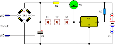
Deriving High Current from 7805 7812 Voltage Regulator Power Supply Citcuits

  1. If, for instance, a power transistor is connected in parallel with the IC, the supply will no longer be protected against short-circuits.
  1. The circuit given here shows that a simpler solution is possible: the power transistor, T1, is provided with an emitter resistor! This effectively solves the problem, because the current through Tl is then proportional to the current supplied by the voltage regulator.
  2. But this solution A suffers from a heavy power loss during short-circuit conditions, which is not really acceptable either.
  3. There are various ways and means of drawing more current from a voltage regulator IC than it was originally intended to supply, but most methods have their disadvantages.
  4. lf the 7805 or 7812 regulator and T1 are mounted onto the same heatsink, the transistor is also thermally protected! The output voltage is dependent only on the type of voltage regulator used and, as drawn here, the circuit is suitable for currents up to 2 A.
  5. lf higher values are required, some components need to be changed according to the table. For currents above 7 A, transistor T1 must be replaced by two parallel-connected transistors each of which has an emitter resistor, R1 and R1 respectively.
  6. That can, of course, be remedied by adding a current sensor in the shape of an extra transistor which, during overload conditions, cuts off the base current to the power transistor. 
Read More..

Yes No Indicator Has Zero Standby Current

This circuit produces a random "Yes" or "No" with a single button press - indicated by the illumination of a red or green LED. The circuit has two advantages over similar circuits. First, it uses just a single momentary contact pushbutton, so no on-off switch is required. When the pushbutton is pressed, an oscillator comprising the 10nF capacitor and 22kΩ resistor at pins 1 & 2 is almost immediately stopped by FET Q1, which pulls the oscillators timing capacitor to the positive rail. However, the 220nF capacitor and 470kΩ resistor in the gate circuit of Q1 introduce a tenth of a seconds delay, so that about 250 oscillations take place before the clock is stopped.

Due to variations in charge on the circuits capacitors, as well as voltage and temperature variations, and the unpredictability of when the pushbutton will be pressed, randomness is assured. The circuit has a high degree of randomness because it takes advantage of a near-perfect complementary square waveform at pins 10 and 11 of the 4047 IC. The oscillator frequency (available at pin 13) is passed through an internal divide-by-2 circuit in the 4047. This appears at pin 10 (Q), and is inverted at pin 11 (Q-bar), thus assuring a near perfect 50:50 duty cycle for the two LEDs.

Circuit diagram:
yes-no-indicator-has-zero standby current
Yes-No Indicator Circuit Diagram
Note:
However, that the "impartiality" of the circuit is partly contingent on the value of the 10nF capacitor and on a reasonably equal current flow through both LEDs. Over five trials, the Yes-No Indicator scored 142 Yes, 158 No, with Yes falling behind No in the fourth trial. Because the circuit only works while switch S1 is pressed, standby current is zero, therefore a miniature 12V battery may be used to power it. In this case the circuit could be used thousands of times before the battery would run flat. The circuit has a further potential use. If the LEDs are omitted and a piezo (capacitive) sounder is wired directly to pins 10 and 11, it will produce a loud beep when equipment is turned on, and will continue to draw less than 0.5mA until it is switched off. The frequency of the beep may be changed by altering the value of the 10nF capacitor and its duration by altering the value of the 220nF capacitor.


Author: Thomas Scarborough - Copyright: Silicon Chip Electronics
Read More..

Simple Electronic Door Lock Circuit Diagram

Its easy to build and straight forward. This electronic door lock has a remarkable conception because it uses only one active component. How does it work?

Electronic Door Lock Circuit Diagram


Simple Electronic Door Lock  Circuit Diagram

To put the relay in tension the 4 buttons S1 – S4 must be pressed. If anyone of the 4 butoons S5 – S8 are pushed the relay doesn’t switch. The supply voltage must be equal to the working voltage of the relay. One transistor like BD135 can switch up to 0.5A, at the same time 2N2222 can do only 0.2A.
Read More..

Simple CD Player Adapter For Car

Whenever Im in the car listening to my favourite CD, it always happens; my batteries go dead. To solve that problem, I built this extremely simple regulator circuit. It steps down the 12V from the lighter socket to 9V which is used by the CD player. Different CD players (I have a Sony Discman) may require different voltages, so just use the correct regulator. All the 78xx series regulators have the same pin out, so the circuit is universal.


Part           Total Qty.                     Description

C1                      1                        1000uF 25V Electrolytic Capacitor   
C2                      1                        10uF 25V Electrolytic Capacitor   
C3                      1                        1uF 15V Elextrolytic Capacitor   
C4                      1                        0.1uF 15V Electrolytic Capacitor   
U1                      1                        7809 Or Other Regulator (See "Notes")    See Notes
MISC                  1                        Cigarette Lighter Plug, Plug For CD Player (See "Notes"),      Heat Sink For U1, Wire, Case.   
   
Notes
  • The voltage your CD player needs will determine which regulator you use. For 9V, use the 7809. For 6V, use the 7806. For the unlikely 5V use the 7805. Remember that whatever regulator you use, you will need to heat sink it. The metal case or metal cover on the case makes a great heat sink.
  • I built the circuit in a small case with the long wire to the cigarette lighter plug coming out one end, then another, slightly shorter wire going out the other end to the CD player.
  • Triple check your wiring. You would hate to ruin an expensive CD player because you reversed one of the connections or hooked the regulator up backwards. Link
Read More..

Heat Sensitive Switch Circuit Diagram

Heat Sensitive Switch Circuit Diagram. At the heart of this heat-sensitive switch is IC LM35 (IC1), which is a linear temperature sensor and linear temperature-to-voltage converter circuit. The converter provides accurately linear and directly proportional output signal in millivolts over the temperature range of 0°C to 155°C. It develops an output voltage of 10 mV per degree centigrade change in the ambient temperature. Therefore the output voltage varies from 0mV at 0°C to 1V at 100°C and any voltage measurement circuit connected across the output pins can read the temperature directly. The input and ground pins of this heat-to-voltage converter IC are connected across the regulated power supply rails and decoupled by R1 and C1. Its temperature-tracking output is applied to the non-inverting input (pin 3) of the comparator built around IC2. The inverting input (pin 2) of IC2 is connected across the positive supply rails via a voltage divider network formed by potentiometer VR1. Since the wiper of potentiometer VR1 is connected to the inverting input of IC2, the voltage presented to this pin is linearly variable. 

Circuit diagram :
Heat Sensitive Switch  Circuit Diagram Heat Sensitive Switch  Circuit Diagram

This voltage is used as the reference level for the comparator against the output supplied by IC1. So if the non-inverting input of IC2 receives a voltage lower than the set level, its output goes low (approximately 650 mV). This low level is applied to the input of the load-relay driver comprising npn transistors T1 and T2. The low level presented at the base of transistor T1 keeps it nonconductive. Since T2 receives the forward bias voltage via the emitter of T1, it is also kept non-conductive. Hence, relay RL1 is in de-energised state, keeping mains supply to the load ‘off’ as long as the temperature at the sensor is low. Conversely, if the non-inverting input receives a voltage higher than the set level, its output goes high (approximately 2200mV) and the load is turned ‘on.’ This happens when IC1 is at a higher temperature and its output voltage is also higher than the set level at the inverting input of IC2. So the load is turned on as soon as the ambient temperature rises above the set level. 

Capacitor C3 at this pin helps iron out any ripple that passes through the positive supply rail to avoid errors in the circuit operation. By adjusting potentiometer VR1 and thereby varying the reference voltage level at the inverting input pin of IC1, the temperature threshold at which energisation of the relay is required can be set. As this setting is linear, the knob of potentiometer VR1 can be provided with a linear dial calibrated in degrees centigrade. Therefore any temperature level can be selected and constantly monitored for external actions like turning on a room heater in winter or a room cooler in summer. The circuit can also be used to activate emergency fire extinguishers, if positioned at the probable fire accident site. The circuit can be modified to operate any electrical appliance. In that case, relay RL1 must be a heavy-duty type with appropriately rated contacts to match the power demands of the load to be operated.


Author : M.K. Chandra Mouleeswaran & Miss Kalan Priya - Copyright :  EFY
Read More..

Automatic Car Alarm

Even the best car alarm is useless if you forget to set it upon leaving your car, whence this circuit. The relay has a make and a break contact: the  former is necessary to delay the switching in of the  alarm after you have got out of your car, and the  latter serves to switch on the car alarm proper. Immediately on re-entering your car, you must press the hidden switch, Si. This causes silicon-controlled rectifier Thi to conduct so that the relay is energized. At the same time, the green LED lights to indicate that the alarm is switched off.  

Circuit diagram :
Best Automatic Car Alarm-Circuit Daigram
 Best Automatic Car Alarm Circuit Diagram

As soon as the ignition is switched off, T, is off, T2  is on, and the buzzer sounds. At the same time,  monostable IC1 is triggered, which causes T3 to  conduct and the red LED to light. The silicon- controlled rectifier is then off, and D4 is reverse  biased, but the relay remains energized via its make  contact for a short time, preset by Pi As soon as this  time has lapsed, the relay returns to its quiescent  state, and the alarm is set via the break contact. The  delay time can be set to a maximum of about 1 minute.
Read More..

Simple Battery Charger Vehicle Circuit Diagram

Unlike many boots, this battery charger continuously charges the maximum current, decreasing only near full battery voltage. In this case the full load current source, transformer / rectifier was 4.4A. It tapers to 4A 13.5V, 14.0V 3A, 2A 14.5V and 15.0V in 0A.


Simple Battery Charger Vehicle Circuit Diagram

Simple Battery Charger Vehicle Circuit Diagram


Parts:

Resistors
R1 = 0.32R
R2 = 8.2R Capacitors
C1 = x 10,000 uF 63V
D1 = 1N4004
D2 = 1N4004
D3 = 1N4004
Q1 = MJ1504
IC REG = 7815
BR1 = 1N4004x4
B1 = 12 Volt Battery
TR 20 volts AC

R1 and R2 are as high power resistor 2W, 3W, 5W or higher. Q1 and IC requires a heatsink good. If they are mounted on the same heatsink and will decrease the circuit turns Q1 gets too hot.
Read More..

Lighting Garden with Solar Energy Circuit Diagram

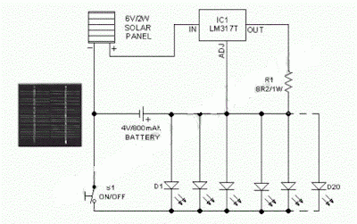
This is an economic circuit of a mini solar lighting system, solar panel 6V/2W is used to charge a rechargeable 4V/800mAh through a current limiting circuit load that uses a LM317T adjustable regulator 3 pin (IC1). Assuming a sunny day 6 hours, a panel will enviarr 2 watts for approximately 900mAh battery. The current can be reduced by increasing the value of R1, for example, 8.2 to 10 ohms ohms.

 Lighting Garden with Solar Energy Circuit Diagram

Lighting Garden with Solar Energy Circuit Diagram


Spec of a typical solar panel 

6V/2W:Maximum power (Pm): 
2WWorking Voltage (Vmp): 
9VWorking Current (Imp): 
220mAOpen Circuit Voltage (Voc): 
10.5VPower Tolerance: -3% to 5%
Read More..

Simple 1KHz Sine wave Generator Circuits Diagram

This simple circuit generates a good 1KHz sine wave adopting the inverted Wain bridge configuration (C1-R3 & C2-R4). It features a variable output, low distortion and low output impedance in order to obtain good overload capability. A small filament bulb ensures a stable long term output amplitude waveform. 

1KHz Sine wave Generator Circuits Diagram

 Notes:
  • The bulb must be a low current type (12V 40-50mA or 6V 50mA) in order to obtain good long term stability and low distortion.
  • Distortion @ 1V RMS output is 0.15% using a 12V 40mA bulb, raising to 0.5% with a 12V 100mA one.
  • Using a bulb differing from specifications may require a change of R6 value to 220 or 150 Ohms to ensure proper circuits oscillation.
  • Set R5 to read 1V RMS on an Audio Millivoltmeter connected to the output with R7 rotated fully clockwise, or to view a sinewave of 2.828V Peak-to-Peak amplitude on the oscilloscope.
  • With C1, C2 = 100nF the frequency generated is 100Hz and with C1, C2 = 1nF frequency is 10KHz but R5 requires adjustment.
  • High gain transistors are preferred for better performance.

Parts:

R1____________5K6  1/4W Resistor
R2____________1K8  1/4W Resistor
R3,R4________15K   1/4W Resistors
R5__________500R   1/2W Trimmer Cermet
R6__________330R   1/4W Resistor
R7__________470R   Linear Potentiometer
 
C1,C2________10nF  63V Polyester Capacitors
C3__________100µF  25V Electrolytic Capacitor
C4__________470nF  63V Polyester Capacitor
 
Q1,Q2_______BC238  25V 100mA NPN Transistors
 
LP1___________12V  40mA Filament Lamp Bulb (See Notes)
 
J1__________Phono chassis Socket
 
SW1__________SPST  Slider Switch
 
B1_____________9V  PP3
 
Clip for 9V PP3 Battery

Read More..

Simple 12V to 250V Converter

A very simple portable 12v to 250V converter can be designed using this circuit diagram. This 12 to 250V converter is designed for portable use with a 12 V car battery.A built astabil multivibrator T1 and T2 generates a rectangular wave at a frequency of 50 Hz. As T1 and T2 drive alternative exit stage system also works in "push-pull". When T1 lead by passing a current T3: T5 and that it engages the latter transistor connects to a half battery of 12 V secondary winding of the transformer Tr When T2 network drive, T6 transistor coupled to the battery the other half of the network adapter.


 If it is used for output stages 40 411 RCA transistors, the current through secondary winding can be up to 10 A, giving a power output of 180 watts. If you use 2N3055 transistors, power output will be about 90 watts. Since the output transistors are driven to saturation, they have very high mounted radiators.Although circuit is simple construction and has high efficiency disadvantage is rectangular output voltage which, in the absence of a regulator is dependent on task: small loads, the output voltage is 250 V ac (not working properly for the engine speed control, light dimmers, televisions, hi-fi equipment.
Read More..

A Simple Hybrid Audio Amplifier Circuit

A Simple Hybrid Audio Amplifier Circuit diagram. The debate still goes on as to which are better, valves or transistors. We don’t intend to get involved in that argument here. But if you can’t make your mind up, you should try out this simple amplifier. This amplifier uses a valve as a pre-amplifier and a MOSFET in the output stage. The strong negative feedback makes the frequency response as flat as a pancake. In the prototype of the amplifier we’ve also tried a few alternative components. For example, the BUZ11 can be replaced by an IRFZ34N and an ECC83 can be used instead of the ECC88. In that case the anode voltage should be reduced slightly to 155 V. The ECC83 (or its US equivalent the 12AX7) requires 2 x 6.3 V for the filament supply and there is no screen between the two triodes, normally connected to pin 9. This pin is now connected to the common of the two filaments.

Project Image :
A simple-hybrid-amp-circuit

The filaments are connected to ground via R5. If you’re keeping an eye on the quality, you should at least use MKT types for coupling capacitors C1, C4 and C7. Better still are MKP capacitors. For C8 you should have a look at Panasonic’s range of audio grade electrolytics. P1 is used to set the amount of negative feedback. The larger the negative feedback is, the flatter the frequency response will be, but the smaller the overall gain becomes.
Circuit diagram:
simple-hybrid-amp-circuit-diagram
Simple Hybrid Audio Amplifier Circuit Diagram

With P2 you can set the quiescent current through T2. We have chosen a fairly high current of 1.3 A, making the output stage work in Class A mode. This does generate a relatively large amount of heat, so you should use a large heatsink for T2 with a thermal coefficient of 1 K/W or better. For L1 we connected two secondary windings in series from a 2x18V/225 VA toroidal transformer. The resulting inductance of 150 mH was quite a bit more than the recommended 50 mH. However, with an output power of 1 W the amplifier had difficulty reproducing signals below 160 Hz. The distortion rose to as much as 9% for a signal of 20 Hz at 100 mW. To properly reproduce low-frequency signals the amplifier needs a much larger coil with an iron core and an air gap. This prevents the core from saturating when a large DC current flows through the coil.

Parts layout:
Parts layout

Such a core may be found in obsolete equipment, such as old video recorders. A suitable core consists of welded E and I sections. These transformers can be converted to the required inductor as follows: cut through the welding, remove the windings, add 250 to 300 windings of 0.8 mm enamelled copper wire, firmly fix the E and I sections back together with a piece of paper in between as isolation. The concepts used in this circuit lend themselves very well to some experimentation. 

The number of supply voltages can be a bit of a problem to start with. For this reason we have designed a power supply especially for use with this amplifier (Quad power supply for hybrid amp). This can of course just as easily be used with other amplifiers. The supply uses a cascade stage to output an unstabilised voltage of 170 V for the SRPP (single rail push pull) stage (V1).


PCB layout:
PCB layout

During initial measurements we found that the ripple on this supply was responsible for a severe hum at the output of the amplifier. To get round this problem we designed a separate voltage regulator (High-voltage regulator with short circuit protection), which can cope with these high voltages. If you use a separate transformer for the filament supply you can try and see if the circuit works without R5. During the testing we used a DC voltage for the filament supply. 

Although you may not suspect it from the test measurements (see table), this amplifier doesn’t sound bad. In fact, it is easily better than many consumer amplifiers. The output power is fairly limited, but is still enough to let your neighbours enjoy the music as well. It is possible to make the amplifier more powerful, in which case we recommend that you use more than one MOSFET in the output stage. The inductor also needs to be made beefier. Since this is a Class A amplifier, the supply needs to be able to output the required current, which becomes much greater at higher output powers. The efficiency of the amplifier is a bit over 30%.


Author: Frans Janssens - Copyright: Elektor Electronics
Read More..

Geiger Counter Uses Cockroft Walton Multiplier


The recent tsunami in Japan and the on-going calamity with the Fukushima nuclear power plant has apparently greatly increased sales of radiation meters, not only in Japan but elsewhere around the world. This device will allow an estimation of the level of radioactivity, being sensitive enough for background radiation monitoring or to provide an estimation of the level of radioactivity from sample objects such as Thorium gas mantles in LPG lamps. The circuit is compatible with several Geiger Muller tubes and three types of indication are provided: the good old-fashioned audible click with each discharge, a flashing LED or an analog meter providing a rough average of radiation levels.

Geiger Counter Uses Cockroft-Walton Multiplier
A normal background count in New Zealand with the smaller GM LND712 tube is around 30 counts per minute, while the larger and more-sensitive LND7312 pancake tube will count about four times this figure. Both GM tubes will detect alpha, beta and gamma radiation. Unless the tube is “filtered”, there is no way of knowing just what type of radiation is being detected, although a rough guess can be made. Alpha particles will be stopped by placing a sheet of paper between the tube and the source, Beta particles (electrons) will be stopped with a few layers of aluminium foil and the more lively Gamma rays will need a layer of lead.

The circuit provides a regulated 500V supply for the Geiger Muller tube. This voltage places the tube into its linear operating mode so that a discharge inside the tube will occur when a particle enters through the mica window of the tube and causes the gas to ionise. The very short pulse produced is stretched and used to signal that a discharge has occurred. The power supply consists of an oscillator and small transistor driving the 6V secondary of a 240VAC mains transformer. The stepped up output of the transformer is fed to a Cockroft-Walton voltage multiplier consisting of diodes D3-D7 and the associated 47nF 630V metallised polyester capacitors.

IC1 is a 40106 Schmitt trigger inverter and IC1a is connected as an oscillator running at several hundred hertz. This is buffered by IC1b and fed to the base of NPN transistor Q1 which then drives the abovementioned transformer. IC1c acts as an error amplifier to regulate the high voltage fed to the GM tube. A portion of the DC voltage produced at the junction of diodes D4 & D5 is monitored by a voltage divider consisting of the 4.7MO and 47kO resistors, in combination with trimpot VR1. When the voltage from D5 is below the positive threshold of IC1c, its output will be high and IC1a will be able to oscillate. Hence, the oscillator will pulse on and off, to maintain the 500V set by VR1.

Each time there is a discharge in the GM tube, the resultant current triggers the BT149 SCR which discharges the associated 100nF capacitor and thereby acts as a pulse stretcher to drive the three remaining inverters in IC1. These in turn drive a high-brightness red LED (LED1), a piezo transducer and an analog metering circuit which is based on an old VU meter movement with a scale graduated in counts/minute. The current drain of the circuit is 10mA and a small 9V battery should run the counter for many hours. Warning: do not touch the window of the GM tube. These are very fragile and made of very thin mica, to allow the low-energy alpha particles to pass through. With the LND 712, 200 counts per minute is roughly equivalent to 0.3 micro-seiverts.
Read More..

A Simple Yet Useful Video Switcher

With the cost of security cameras going down, adding a surveillance system for your store, office or home is becoming more practical all the time. However, you might be dismayed at the thought of having to buy a monitor for every camera that’s installed. dedicating a single monitor to a single camera also runs the risk of burning the camera’s image into the phosphor screen of the CRT. If you prefer a single monitor instead of the “NASA-Mission Control” look, you could buy a special monitor that has a video switcher built in. That type of monitor can automatically switch between several camera inputs in sequence.

 Useful Video Switcher Circuit Diagram

Useful Video Switcher


With that type of arrangement, you’d have to watch only one screen instead of having to scan a wall of CRTs. Switching between several cameras would also prevent image burn-in on the monitor. Those types of monitors, unfortunately, are also very expensive, offsetting the cost savings of even the cheapest surveillance camera. Video switchers are also available, but the cost of a switcher and a monitor could be as expensive as a monitor/switcher combination unit. A viable alternative for a video switcher is to build your own. Thanks to some recently introduced ICs, the cost and effort of designing and building such a unit has become both quite affordable and easy.


The video switcher described here can display the output of two, three, or four cameras on a single monitor. The number of cameras is set by a DIP switch on the circuit board. That feature avoids blank displays if less than four cameras are used by sequencing through only the inputs that are connected to a camera. In the automatic mode, the cameras are switched at a rate that can be varied with a panel mounted control. The switching rate can be set from about once per second to about once every 20 seconds. In the manual mode, one camera output is displayed continuously. A momentary-toggle switch is then used to step through the various cameras.

How it works

The heart of the video switcher is a Maxim MAX454. That integrated circuit contains a four-way video multiplexer and an amplifier that operates as a low-impedance line driver. The resulting video output is high quality with very low phase distortion. The video inputs are selected by applying a binary number to the address inputs. The binary number is also used to light a series of LEDs that indicate whichh camera input is currently selected. The circuit is powered by a 9-volt AC wall-adapter transformer, two diodes, and two voltage regulators.

Circuit description

Figure 1 is a schematic diagram of the video switcher. Multiplexer IC1 has four video inputs, two address inputs, one video output, one external amplifier input, and and three power terminals. The video cameras connect to the video inputs through J1-J4. The inputs are terminated with 75 ohm resistors R1-R4. The gain of the internal video amplifier is set by a feedback network connected to pin 13 of IC1. That feedback network consists of R5-R8 and C3. The gain is set to 2 in order to compensate for any loss through the 75 ohm terminator resistor, R9. The resulting net gain is 1 at output J5.

The binary addressing circuit is built around IC2, a CD4017 decade counter. That chip produces one positive output at a time on each of its ten outputs in sequence for every clock pulse. The first four outputs at pins 3,2,4,and 7 are connected to transistors Q1- Q4. Those transistors drive LED1-LED4 through current limiting resistor R15. The outputs from IC2 (pins 2,4, and 7) are also decoded into binary logic by diodes D1-D4. The binary logic is sent to the address input lines of IC1.


The number of cameras connected to the video switcher is set with S1. Each switch in S1 is connected to an output from IC2. If, for example, there are only two cameras connected to the video switcher, S1-a is closed. That connects the third output to IC2’s reset line. When IC2 advances to the third count, that output passes through S1-a to the reset, and IC2 resets to zero, activating the first camera. The sequence would be camera 1, camera 2, then back to camera 1. Closing S1-b or S1-c instead of S1-a will let the video switcher cycle through three or four cameras, respectively.

Clock pulses for the counter are generated by IC3, an LMC555 CMOS timer. The pulse rate and pulse width is controlled by C4, R10, R11 and potentiometer R12. By adjusting R12, the output frequency of IC3 can be controlled between 1 Hz and 1/20 Hz. The clock pulses from IC3 are connected to IC2 through S2, a three position toggle switch. Switching S2 to the auto position lets the pulses from IC3 select the next camera at a rate set by R12. When S2 is in its center-off position, no switching takes place, and whatever camera input is selected is passed through to the output.


The select position on S2 is a momentary contact. That position raises the clock input of IC2 to 5 volts, which increments the binary count and selects the next camera. When S2 is released, it springs back to its center-off position. The clock input of IC2 is then held at a low-logic level by R13. The MAX454 requires ±5 volts while the other ICs require only +5 volts. Power is supplied by AC adapter T1, rectifier diodes D5 and D6, regulators IC4 and IC5, and filter capacitors C6-C9.

Construction

Because of the high frequency video signals involved, the video switcher should be built on a printed circuit board. The circuit is simple enough to fit onto a single-sided board with only two jumpers needed. A foil pattern is included for etching and drilling your own board. Alternatively, an etched board can be purchased from the source given in the parts list. A feature of that board design is ground traces that run between all of the video signal traces in order to keep induced noise and crosstalk between the signals to a minimum.

Weather you etch a board from the foil pattern or purchase one from the source in the parts list, use the parts-placement diagram in fig. 2 for component placement. It is easiest to install and solder the resistors and diodes first. Once those components are in place, scrap component leads can be used for the two jumper wires. Next, install S1 and sockets for IC2 and IC3. Do not use a socket for IC1, the MAX454 multiplexer.

When installing J1-J5, hold the connectors tight against the board while soldering the center pin. The assembly can then be placed on a heat-resistant surface and the ground pins soldered. Because of their size and mass, a larger soldering iron might be needed to solder J1-J5. Otherwise the board might be damaged if heat is applied too long. Once the connectors are soldered in place, Q1-Q4, IC4, IC5, and all the capacitors can be installed. The LEDs should be installed next, leaving their leads long so that they can be bent to reach through the front panel of the enclosure.

Double-check the orientation of the polarized components, so that they are not installed backwards by accident. Once a component is soldered in place, removing it becomes much more difficult. Solder two 3-inch long wires onto the two terminals of R12 that are clockwise when viewing the potentiometer from the back. Connect those wires to the holes for R12 on the board. Three additional 3-inch long wires are soldered onto the terminals of S2. The center terminal connects to the hole near C5 and R13.

The momentary-contact terminal connects to the hole near R14. The remaining terminal connects to the hole near IC3 and R10. Solder IC1 directly onto the circuit board. That will result in the shortest possible lead length for the video signals. Plug IC2 and IC3 into their sockets, being careful to handle them as static-sensitive CMOS devices. Solder the T1 leads onto the board. Examine the board for any wiring errors, bad solder joints, and incorrect components. Once the assembly is inspected, it can be tested.

Testing

Plug T1 into an AC outlet and measure the voltages across C8 nd C9. The voltage across C8 should measure +5 volts. Across C9, the voltage should be -5 volts. To select two cameras, set S1-a on; to select three cameras, set set S1-b on; and to select all four cameras, set S1-c on. Only one switch at a time should be on. When switch S2 is toggled to its momentary position, the LEDs should sequence to the next indicator each time S2 is toggled. The order of the LEDs should cycle from 1 through 4 and repeat. When S2 is set to automatic, the LEDs should automatically at a rate that should vary as potentiometer R12 is adjusted. Connect cameras to J1-J4 and a monitor to J5.

The video signal on the monitor should switch from camera to camera according to the LEDs. After testing is completed, drill appropriate holes in a suitable enclosure for J1-J5, LED1-LED4, S2, and R12. Mount the board in the enclosure using the mounting hardware for J1-J5 to hold it in place. Mount R12 and S2 in the front panel and bend the LEDs so they fit through the holes in the panel. The hole for the T1 wire should be drilled at a point where the two halves of the enclosure meet.

Tie a knot in the wire for strain relief and place the wire in the enclosure hole with the knot on the inside of the enclosure before closing the case. That completes the project. If all has gone well, as is likely, your video switcher is now ready for use.

SEMICONDUCTORS
  • IC1 - MAX454 multiplexer, integrated circuit (MAXIM)
  • IC2 - CD4017 decade counter, integrated circuit
  • IC3 - LMC555 timer, integrated circuit
  • IC4 - 78l05 voltage regulator, integrated circuit
  • IC5 - 79l05 voltage regulator, integrated circuit
  • Q1-Q4 - MPSA14, NPN transistor
  • D1-D4 - 1N914, silicon diode
  • D5, D6 - 1N4004, silicon diode
  • LED1-LED4 - Light emitting diode, red
RESISTORS
  • R1-R4, R9-R15 - 75 ohm
  • R5 - 150,000 ohm
  • R6 - 620 ohm
  • R7 - 1100 ohm
  • R8 - 1000 ohm
  • R10 - 10,000 ohm
  • R11 - 51,000 ohm
  • R12 - I megohm potentiometer, panel mount
  • R13, R14 - 100,000 ohm
CAPACITORS
  • C1,C2,C5 - 0.1mF, 50WVDC, metalized film
  • C3 - 6.8 pF, ceramic disc
  • C4 - 10 mF, 50 WVDC, low leakage electrolytic
  • C5, C7 - 470 mF, 25 WVDC, electrolytic
  • C8, C9 - 100 mF, 16 WVDC, electrolytic
ADDITIONAL PARTS AND MATERIALS
  • S1 - DIP switch, 3 position
  • S2 - Toggle switch, single pole double throw, one momentary position
  • J1-J5 - Video connector, chassis mount, “F” type
  • T1 - 9 volt AC wall adapter transformer, PC board, IC sockets, LED holders, 22 gauge hookup wire, knob, enclosure, hardware, etc.
Read More..

Supper Deluxe Charge Rate Limiter for Small Capacity NiCad Batteries

Here is a deluxe version of the simple charge rate limiter, using the same idea but with the ability to charge two packs simultaneously from a single wall charger. For circuit description and parts list, see the simple charger page. Since wall chargers provide about 55mA, you should not use this dual circuit to charge batteries at rates greater than 27mA (for a total of 54mA).

Read More..

Loudspeaker Impedance Meter

Also suitable for Headphones Operates in conjunction with a DVM . A simple Impedance Meter can be useful to measure the actual impedance a loudspeaker or headphone is presenting @ 1kHz standard frequency. The circuit, designed on request, relies on an earlier design (Spot-frequency Sine wave Generator) to obtain a stable, low distortion 1kHz sine wave avoiding the use of thermistors, bulbs or any special amplitude-limiting device. The sine wave output, after some amplitude setting obtained by means of P1, is sent to the device under measurement through a resistor.

A regulated supply is necessary to obtain a stable output waveform. D1 and D2 force IC1 to deliver 6.2V output instead of the nominal 5V. The measurement is done in two stages: as a constant current supply of the device under test is necessary, this can be set at first by adjusting P1 and measured across the series resistor (R7 or R8, depending on the impedance value to be measured); then, the meter is switched across the device under test and the actual impedance will be read directly on the meter display.
Circuit diagram:
Loudspeaker Impedance Meter Circuit DaigramLoudspeaker Impedance Meter Circuit Diagram 
Parts:
P1_______________4K7  Linear Potentiometer
R1______________12K 1/4W Resistor
R2_______________2K2 1/4W Resistor
R3_______________1K 1/2W Trimmer (Cermet)
R4_______________1K5 1/4W Resistor
R5_______________4K7 1/4W Resistor
R6_______________3K3 1/4W Resistor
R7_____________100R 1/4W Resistor (See Notes)
R8_______________1K 1/4W Resistor (See Notes)
R9_______________1K 1/4W Resistor (Optional)
C1______________22nF 63V Polyester Capacitor
C2_____________330nF 63V Polyester Capacitor
C3______________22µF 25V Electrolytic Capacitor
D1,D2_________1N4148 75V 150mA Diodes
D3_______________3mm Red LED (Optional)
Q1,Q2,Q3_______BC550C 45V 100mA Low noise High gain NPN Transistors
IC1____________78L05 5V 100mA Regulator IC
SW1,SW2_________SPDT Toggle or Slider Switches
SW3_____________SPST Toggle or Slider Switch
B1________________9V PP3 Battery

Clip for PP3 Battery
Circuit set-up using an oscilloscope:

Connect the oscilloscope in place of the DVM and rotate P1 fully clockwise.
Short the speaker output and adjust R3 to obtain a sine wave of about 2.2V peak-to-peak amplitude.

"By ear" circuit set-up:

Connect a small loudspeaker or one of the two earpieces forming a pair of headphones to the circuit output and rotate P1 to obtain a moderate output sound level.

Carefully adjust R3 until the output sound will stop; then turn back the trimmer very slowly and stop adjusting immediately when the sound will start again.

Measurement:
  • Connect a Digital Voltage Meter set to 200mV ac range to the DVM output terminals
  • Connect the device under test to the Speaker terminals
  • Switch SW1 in the position towards R7 if the impedance value to be measured is below 100 Ohm or towards R8 if above
  • With SW2 in the "Set" position power-on the circuit by means of SW3
  • Adjust P1 in order to read exactly 100.0mV on the DVM display
  • Switch SW2 in the "Measure" position and read directly the loudspeaker or headphones impedance value on the DVM display, e.g. 8.5mV = 8.5 Ohm
  • Please note that when measuring devices with impedance values above 100 Ohm (SW1 set towards R8), the decimal point in the DVM reading must be ignored. E.g. if the display shows 70.5mV, the impedance will be 705 Ohm

Notes:
  • For very precise measurements use 1% or 2% tolerance resistors for R7 and R8.
  • D3 LED pilot light and its current limiting resistor R9 are optional.
Read More..

How to Using Diodes as a photosensor Circuit diagram

Using Diodes as a photosensor

A photodiode is a PN junction or PIN structure that when light reaches the junction, it excites an electron thereby creating a free electron positively charged. This mechanism is also known as the photoelectric effect, common in transistors, diodes and ICs are made ​​of semiconductors, and contain PN junctions. Almost all of the potentially active constituents are a photodiode and may be used as a photosensor. The PN junction needs to be exposed to light, so to use a semiconductor diode as a light bulb must have a transparent glass, these diodes with these characteristics can be used to measure the light intensity.


 Circuit diagram of a light intensity meter with diode.

Circuit diagram of a light intensity meter with diode.
 

a test circuit diode light sensor

List of components:
D1 1n148 or any other photo-sensitive element
T1, T2 BC548 or similar
C1 680n
R1 2M

Above this circuit that is very popular, it works with LEDs, photodiodes and photo-resistors. V is a voltmeter which can be a multimeter.

sourced by www.circuitsstream.
Read More..

Bridge Rectifier LED Indicator

Using a few diodes and a LED, you can make a nice indicator as shown in associated schematic diagram that can be used for a lot of applications (with a bit of luck). It’s quite suitable for use in series with a doorbell or thermostat (but don’t try to use it with an electronically con-trolled central-heating boiler!). This approach allows you to make an attractive indicator for just a few pennies.

Bridge-Rectifier-LED-Indicator image

The AC or DC current through the circuit causes a voltage drop across the diodes that is just enough to light the LED. As the voltage is a bit on the low side, old-fashioned red LEDs are the most suitable for this purpose. Yellow and green LEDs require a somewhat higher forward voltage, so you’ll have to first check whether it works with them. Blue and white LEDs are not suitable. You also don’t have to use modern high-efficiency types (sometimes called ‘2-mA LEDs’ or ‘3-mA LEDs’). If a DC current flows through the circuit and the LED doesn’t light up, reverse the plus and minus leads.

Circuit diagram :

Bridge-Rectifier-LED-Indicator-Circuit-Diagram

Bridge-Rectifier  LED Indicator Circuit Diagram

When building the circuit, you’ll notice that despite its simplicity it involves fitting quite a few components to a
small printed circuit board or a bit of prototyping board. That’s why we’d like to give you the tip of using a bridge rectifier, since that allows everything to be made much more compact, smaller and more tidy, and it eliminates the need for a circuit board to hold the components. Besides that, you can surprise friend and foe alike, because even an old hand in the trade won’t understand the trick at first glance and will likely mumble something like “Huh?
That’s impossible.”

A bridge rectifier contains four diodes, which is exactly what you need. If you short the + and – terminals of the bridge, you create a circuit with two pairs of diodes connected in parallel with oppo-site polarity. Select a bridge rectifier that can handle the current that will flow through it. In the case of a doorbell, for example, that can easily be 1 A. Select a voltage of 40 or 80 V.

Never use this circuit in combination with mains voltage, due to the risk of contact with a live lead. 


Ecircuitslab.com
Read More..

Garage Door Closing Circuit Just using Relays

Because I’m old school, I wanted to build a Garage Door Closing circuit without relying on integrated configurations (555 timer etc) to keep it simplistic. The circuit closes the garage door after two minutes with C3 and four minutes with the addition of C2. The timer relay is surprisingly accurate (+/- five seconds). Another feature is to ensure that the garage door actually did close, such as if it’s stopped mid-operation by the user.


Garage Door Closing Circuit Just using Relays

Description:

S3 (magnetic N.C.) is located at the garage door and activates the circuit when the garage door opens.
RL1 is the reset timer. It’s maintained in the “on” position for two minutes by C3 while the trigger capacitor, C4, is charged. RL2 is the conduit, directing C4 to either RL3 or R1 to ground when off. Purpose of R1 is to prevent arching across contacts and a fast discharge. RL3’s contacts are connected to the Garage Door’s Momentary Switch and is sustained “on”  for a half second by C5.

When C3 discharges to the cutoff voltage of RL1, it turns off and resets. C4 charges C5, which turns on RL3 and initiates the garage door. Because C4 does not have the time to fully discharge, it should be at least three times the value of C5. If it does not close, RL1 in countdown mode will reset and open the door. When it resets again, the door will close.

Turning off the circuit, C1 maintains RL1 “on” slightly longer to ensure that RL2 is set to discharge C4 to R1. If this is not done and C4 is not discharged, the garage door will not open until it discharges naturally and falls below the trigger voltage for RL3.  The circuit would be useless for several days.

Garage Door Closing Circuit Just using Relays

Notes:

  • Time delay of RL1 after reset drops 15 seconds because of the short charge time.
  • To boost RL3 to a one-second delay, increase C5 to 1000uF.
  • D2, D3, and D4 isolate the crucial sections of the circuit.
  • Relays do not turn off at the same rate. I conducted a test by tripping the circuit on and off at a high rate and discovered the possibility of C4 turning on RL3. The addition of C1 solved this.
Author: Roland Segers (speedmail-at-gmail.com)
Read More..

Traffic Interactive Educational Circuit Diagram

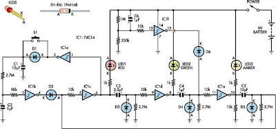
This is a circuit of an educational interactive traffic, it uses a single Schmitt-trigger inverter IC (IC1a-IC1f) to directly drive three LEDs (red, green and yellow). When you call, the circuit turns red for 30 seconds, then green for 6 seconds, then yellow for 3 seconds, then repeats the sequence.

Interaction of Light is provided by S1 which shortens the red to a period of just over 3s, if pressed while red is on.

Traffic Interactive Educational Circuit Diagram

Traffic Interactive Educational Circuit Diagram

Read More..

Test Transmitter for Radio Control Circuit Diagram

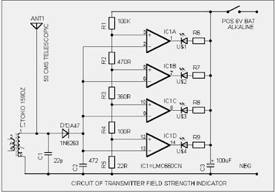
This circuit is ideal for those with radio transmitting equipment in the control frequency of 35 or 40 MHz, it is a field strength meter, it can check the output power of the transmitters, so you can detect any problems even before the equipment is used. For the test and verification of the correct operation of the transmitter R / C, it must 3 or 4 LEDs lit at a distance of 10 meters. 

The length adjustment of the antenna will allow the gauge to operate at a shorter distance.L1 must be initially set to the maximum number of lighting LEDs in a distance of 10 meters or more. Toko coil used in the circuit is no longer manufactured but the coil can be constructed at a frequency of 40Mhz.

Test Transmitter for Radio Control Circuit Diagram

Test Transmitter for Radio Control Circuit Diagram

Read More..

Tiny Metronome Circuits Diagram

Tiny  Metronome Circuits Diagram

Tiny  Metronome Circuits Diagram

Notes:

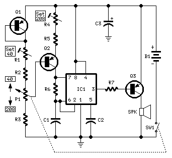
  • Q1 & Q2 provide linear frequency operation of IC1 following P1 resistance variation.
  • Q3 was added in order to obtain a louder click, similar to clockwork metronomes.
  • A 12V micro battery was used to obtain a higher output power and more compactness.
  • Rotate P1 fully towards R2, then set R1 to obtain 40 beats per minute (compare with another metronome).
  • Rotate P1 fully towards R3, then set R4 to obtain 208 beats per minute.
  • Finally mark the entire scale with the usual metronome steps, as follows:
    40 - 42 - 44 - 46 - 48 - 50 - 52 - 54 - 58 - 60 - 63 - 66 - 69 - 72 - 76 - 80 - 84 - 88 - 92 - 96 - 100 - 104 - 108 - 112 - 116 - 120 - 126 - 132 - 138 - 144 - 152 - 160 - 168 - 176 - 184 - 192 - 200 - 208.

Parts:

P1______100K   Linear Potentiometer
 
R1_______10K   1/2W Trimmer Cermet
R2_______10K   1/4W Resistor
R3______330K   1/4W Resistor
R4_______50K   1/2W Trimmer Cermet
R5______100K   1/4W Resistor
R6,R7_____1K   1/4W Resistor
 
C1________1µF   63V Polyester Capacitor
C2_______10nF   63V Polyester Capacitor
C3_______47µF   25V Electrolytic Capacitor
 
IC1_____NE555   General purpose timer IC
 
Q1,Q2___BC560C  45V 100mA Low noise High gain PNP Transistors
Q3_____ZTX753  100V 2A PNP Transistor
 
SW1______SPST Switch (Ganged with P1)
 
SPK______8 Ohm 40mm. Loudspeaker 
 
B1_____12V Battery (MN21, GP23A or VR22 type)
Read More..

Simple Horn Bugle Electronic Circuit Diagram

This Simple Horn Bugle Electronic Circuit Diagram just a door trigger input 4093, bound in a low frequency oscillator, as the transistor Q1, which is the IRF511 FET amplifier is directly connected to a small speaker with horn. The output frequency can be changed by adjusting potentiometer R1.


Simple Horn Bugle Electronic Circuit Diagram

Simple Horn Bugle Electronic Circuit Diagram

Read More..

Bathroom Fan Controller

Many bathrooms are fitted with a fan to vent  excess humidity while someone is showering. This fan can be connected to the light  switch, but then it runs even if you only want  to brush your teeth. A better solution is to  equip the fan with a humidity sensor. A disadvantage of this approach is that by the time  the humidity sensor switches on the fan, the  room is already too humid. Consequently, we decided to build a circuit  that operates by sensing the temperature of  the hot water line to the shower. The fan runs  as soon as the water line becomes hot. It continues to run for a few minutes after the line  cools down, so that you have considerably  fewer problems with humidity in the bathroom without having the fan run for no reason.

Naturally, this is only possible if you can  fit a temperature sensor somewhere on the  hot water line and the line does not become  warm if hot water is used somewhere else. We use an LM335 as the temperature sensor.  It generates an output voltage of 10 mV per  Kelvin. The output voltage is 3.03 V at 30 °C,  3.13 V at 40 °C, 3.23 V at 50 °C, and so on.  We want to have the fan switch on at a temperature somewhere between 40 and 50 °C (approx.100–150 °F). To do this accurately,we first use the opamps in IC2 to improve  the control range. Otherwise we would have  an unstable circuit because the voltage differences at the output of IC1 are relatively  small. IC2a subtracts a voltage of exactly 3.0 V from  the output voltage of IC1.

Circuit diagram :
Bathroom-Fan-Controller-Circuit -Diagram
 Bathroom Fan Controller Circuit Diagram

It uses Zener diode  D1 for this purpose, so this is not dependent on the value of the supply voltage. The  value of R2 must be selected according to  the actual supply voltage so that the current through D1 is approximately 5 mA. It is  600 Ω with a 6-V supply (560 Ω is also okay),  or 2400 Ω (2.2 kΩ) with a 15-V supply. If you  have to choose between two values, use the  lower value. IC2b amplifies the output voltage of IC2a  by a factor of 16 ((R7 + R8) ÷ R8). As a result,  the voltage at the output of IC2b is 0.48 V at  30 °C, 2.08 V at 40 °C (104 °F), and 3.68 V at  50 °C (122 °F). Comparator IC3a compares this  voltage to a reference voltage set by P1. Due  to variations resulting from the tolerances of  the resistor values, the setting of P1 is best  determined experimentally. A voltage of 2.5 V  on the wiper should be a good starting point  (in theory, this corresponds to 42.6 °C).

When  the water line is warm enough, the output of IC3 goes Low. R10  provides  hysteresis  at  the  output  of  IC3a by pulling the voltage on the wiper of  the setting potentiometer down a bit when  the output of IC3a goes Low. IC3b acts as an  inverter so that relay Re1 is energised via T1,  which causes the fan to start running. After  the water line cools down, the relay is de-energised and the fan stops. If this happens  too quickly, you can reduce the value of R11  (to 33 kΩ, for example). This increases the  hysteresis. The circuit does not draw much current, and  the supply voltage is noncritical. A charging  adapter from a discarded mobile phone can  thus be used to power the circuit. If the supply voltage drops slightly when the relay is  energised, this will not create any problem.  In this case the voltage on the wiper of P1 will  also drop slightly, which provides a bit more  hysteresis on IC3a.

Author : Heino Peters - Copyright : Elektor
Read More..

Build a Metal Detectors CCO schematic Diagram

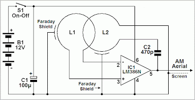
This is a schematic of a simple metal detector that uses technology CCO, by Coil Coupled Operation. Thomas Scarborough designed this new incarnation of the metal detector, a new genre that he invented in 2004. This is the first project of the Internet and can be built easily.  


 Metal Detectors CCO Schematic Diagram


Metal Detectors BCC schematic Diagram
Read More..

Preamp Stage For Ceramic Phono Cartridge

While we have published a number of variations on a standard RIAA preamplifier for magnetic phono cartridges, we have not published a preamp stage for ceramic phono cartridges. Typically, these were supplied as turnover cartridges in record changers but there were higher quality versions such as the Decca Deram. These phono cartridges are piezoelectric devices which require a very high input impedance. Similarly, violin pick-ups made by Fishman, Barcus Berry and others are piezo devices. These two circuits have been requested for a violin pickup but could equally well suit a ceramic or crystal pickup. The op amp circuit uses a TL071 connected as a voltage-follower. It can run from a battery supply of ±9V.
Circuit diagram:
preamp-stage-for-ceramic-phono-cartridge-or-violin-pickup

The alternative transistor circuit uses a BC549 connected as an emitter-follower but with bootstrapping of the input bias network to provide a high input impedance. Both circuits have input coupling capacitors but since the transducers are capacitive (ie, piezo) they could possibly be omitted. Both circuits will probably need to be followed by further gain, depending on the output level. For a violin pickup, a parametric equaliser is also recommended, and for this we would suggest the 3-band parametric equaliser published in the July 1996 issue of SILICON CHIP. With a slight change to the feedback of the first op amp in this circuit, the extra gain required could also be provided.

Read More..

Guitar Effect Pedal Power Circuit Diagram


A small box is fitted to the rear of the amplifier providing a 9V output for the effect pedal. The amplifier section gets 9V through a pedal switch. This power output and guitar signal input lines are combined into a single unit with multi-way cable connecting points as shown in the following figure.
Circuit diagram :
Guitar Effect Pedal Power-Circuit Diagram
Guitar Effect Pedal Power Circuit Diagram
The circuit can be divided into two sections: power supply and signal handling. The power supply section is built around transformer X1, regulators 7805 and 7905, bridge rectifier comprising diodes D1 through D4, and a few discrete components. The signal-handling circuit is built around two OP27 op-amps (IC3 and IC4). The power supply of about 9V for the effect pedals is derived from step-down transformer X1. MOV1 is a metal-oxide varistor that absorbs any large spike in mains power.  IC 7905 (IC1) is a -5V low-power regulator. By using a 3.9V zener diode (ZD1) at its ground terminal, you get -8.9V output. The same technique is also applied to IC 7805 (IC2)-a +5V regulator to get 8.9V. Use good-quality components and heat-sinks for the regulators. This supply is more than enough for the five effect pedals.
The greater the voltage drop across the regulator, the lower the output current potential. Resistors R1 and R2 provide a constant load to ensure that the regulators keep regulating. Capacitors C3 through C8 ensure that the supplies are as clean as possible. It is very important to use proper heat-sinks for IC1 and IC2. Otherwise, these could heat up.
Working of the circuit is simple. The input signal stage uses a basic differentiation amplifier to accept the incoming signal and a voltage follower to buffer the output to the power amplifier. The differential amplifier is built around IC3. It works by effectively looking at the signals presented to its inputs. If the input signals are of different amplitudes, IC3 amplifies the difference by a factor determined by R4/R3 (where R4=R6 and R3=R5). If the input signals have same amplitudes, these are attenuated by the common-mode rejection ratio (CMRR) of the circuit. The value of CMRR is determined by the choice of the op-amp the auxiliary components used and circuit topology. You can use standard resistors. With the values shown, you get an overall gain of unity.
The combination of resistor R7 and C13 serves as a passive low-pass filter, progressively attenuating unwanted high-frequency signals. The second op-amp (IC4) forms a simple voltage follower (its output follows its input), providing a low output impedance to drive into the standard power amplifier.  Assemble the circuit on a general-purpose PCB and fit it to the rear of an amplifier. The unit must be compact, yet robust. So use a very sturdy aluminium extrusion for the cabinet in order to neatly house the assembled PCB.
To ensure simple operation, there are only three connections to the unit. First, mains power is tapped from the transformer. The second lead carries the 9V output to the amplifier. The third is the guitar signal input at the five-way socket for connection to the effect pedal. 

Read More..

How to Treble and Bass Control without IC or Transistor

This Treble and Bass Control without IC or Transistor circuit consists of bass and treble just a few capacitors, resistors and two potentiometers to adjust BASS and TREBLE. The circuit is very functional, can be used to adjust the small sound amplifiers. And control Treble and works relatively well. The interesting thing is that this control does not use or IC or transistor.

Treble and Bass Control without IC or Transistor Circuit Diagram


How to Treble and Bass Control without IC or Transistor
Read More..

LED Flasher for Cars and Motorcycles Circuit Diagram

This is a flasher that uses 4 high brightness LEDs that can be used in Automotive, Motorcycle or bicycle. It uses the IC 555 which is a monostable to adjust the flasher you can use the RV1, which can be a potentiometer or trim pot 100k. If built in SMD it fits within the own flashlight.

 LED Flasher for Cars and Motorcycles Circuit Diagram

LED Flasher for Cars and Motorcycles Circuit Diagram

Read More..

Balanced Microphone Preamplifier

The preamplifier is intended for use with dynamic (moving coil–MC) microphones with an impedance up to 200 Ω and balanced terminals. It is a fairly simple design, which may also be considered as a single stage instrument amplifier based on a Type NE5534 op amp. To achieve maximum common-mode rejection (CMR) with a balanced signal, the division ratios of the dividers (R1-R4 and R2-R5 respectively) at the inputs of the op amp must be identical. Since this may be difficult to achieve in practice, a preset potentiometer, P1, is connected in series with R5. The preset enables the common-mode rejection to be set optimally. Capacitor C1 prevents any direct voltage at the input, while resistor R7 ensures stability of the amplifier with capacitive loads.
Circuit diagram:
Balanced_Microphone_Preamplifier_Circuit_Diagramw 
Balanced Microphone Preamplifier Circuit Diagram
Power supply:
Power_Supply_Balanced_Microphone_Preamplifier_Circuit_Diagramw
Power Supply For Balanced Microphone Preamplifier
Resistor R3 prevents the amplifier going into oscillation when the input is open circuit. If the microphone cable is of reasonable length, R3 is not necessary, since the parasitic capacitance of the cable ensures stability of the amplifier. It should be noted, however, that R3 improves the CMR from >70 dB to >80 dB. Performance of the preamplifier is very good. The THD+N (total harmonic distortion plus noise) is smaller than 0.1% with an input signal of 1 mV and a source impedance of 50 Ω. Under the same conditions, the signal-to-noise ratio is –62.5 dBA. With component values as specified, the gain of the amplifier is 50 dB (´316). After careful adjustment of P1 at 1 kHz, the CMR, without R3, is 120 dB. The supply voltage is ±15 V. The amplifier draws a current at that voltage of about 5.5 mA. Note the decoupling of the supply lines with L1, L2, C2–C5.
Read More..