Showing posts with label power. Show all posts

Wednesday, November 12, 2014

FM Power Amplifier 250mW

This project is a simple 2-transistor VHF power amplifier, with about 16dB gain, and requires no tuning or alignment procedures. Wideband techniques have been used in the design and the circuit is equipped with a "lowpass" filter to ensure good output spectral purity. The project has been designed for assembly on a single-sided printed circuit board. The circuit is specifically designed to amplify the output of 7mW to 10mW WBFM transmitters (wide band) to a final level of 250mW to 300mW, after the filter.


Circuit Description
The first stage (Q1) operates in Class-A. Although Class-A is the least efficient mode, it does offer more RF gain than other clases of bias, and Q1 is a low-level stage, when compared to the higher power Q2 stage. The output of this stage is around 70mW of RF power. The stage is
untuned so that it gives a very broadband characteristic. The transistor is biased by means of R5, R6 and L6, and the residual (standing) DC current is set by R4. The input signal is coupled by C9 to the Base of the transistor. Q2 is operated in Class-AB which leads to greater efficiency, but the RF gain is only about 8dB, but it amplifies the output of Q1 to typically 250mW. Q2 is
biased by means of R3, R2 and L4. The input signal from Q1 is coupled to the Base of Q2 via C7.
The voltage regulator Q3 (78L08) is used to regulate the supply voltage to Q1 and the bias votages to both Q1 and Q2 so that the output RF power is relatively constant, even with large variations of supply voltage. Q3 also removes supply ripple as well as providing power for an
FM transmitter like Kit 3018 wireless microphone with the required DC 8v power.

The output of the amplifier is filtered with a low-pass filter to reduce the output spurious and harmonic content. The output filter consists of C3, C4, L1 and L2.

COMPONENTS
Resistors 5%, 1/4W, carbon:
10R R1 brown black black
22R R7 red red black
47R R3 yellow orange black
120R R4 brown red brown
470R R2 yellow violet brown
2K2 R5 red red red
4K7 R6 yellow violet red
2N2369 Q1
2N4427 Q2 1
Ceramic caps
33p C3
47p C4
1n C5 C6 C7 C8 C9
10n C1 C11
Ecaps:
220u/16V C2
10u/25V C10
78L08 Q3
RFC L4 L5 L6
Ferrite L3
3 turn coil L2
5 turn coil L1
2 pole terminal block
HS106 heatsink ( 
Read More..

LM4906 Boomer Audio Power Amplifier circuit and epxlanation

The well-known LM386 is an excellent choice for many designs requiring a small audio power amplifier (1-watt) in a single chip. However, the LM386 requires quite a few external parts including some electrolytic capacitors, which unfortunately add volume and cost to the circuit. National Semiconductor recently introduced its Boomer® audio integrated circuits which were designed specifically to provide high quality audio while requiring a minimum amount of external components (in surface mount packaging only). The LM4906 is capable of delivering 1 watt of continuous average power to an 8-ohm load with less than 1% distortion (THD+N) from a +5 V power supply. The chip happily works with an external PSRR (Power Supply Rejection Ratio) bypass capacitor of just 1 µF minimum.
In addition, no output coupling capacitors or bootstrap capacitors are required which makes the LM4906 ideally suited for cellphone and other low voltage portable applications. The LM4906 features a low-power consumption shutdown mode (the part is enabled by pulling the SD pin high). Additionally, an internal thermal shutdown protection mechanism is provided. The LM4906 also has an internal selectable gain of either 6 dB or 12 dB. A bridge amplifier design has a few distinct advantages over the single-ended configuration, as it provides differential drive to the load, thus doubling output swing for a specified supply voltage. Four times the output power is possible as compared to a single-ended amplifier under the same conditions (particularly when considering the low supply voltage of 5 to 6 volts).Circuit diagram:
Boomer Audio Power Amplifier Circuit Diagram

When pushed for output power, the small SMD case has to be assisted in keeping a cool head. By adding copper foil, the thermal resistance of the application can be reduced from the free air value, resulting in higher PDMAX values without thermal shutdown protection circuitry being activated. Additional copper foil can be added to any of the leads connected to the LM4906. It is especially effective when connected to VDD, GND, and the output pins. A bridge configuration, such as the one used in LM4906, also creates a second advantage over single-ended amplifiers. Since the differential outputs, Vo1 and Vo2, are biased at half-supply, no net DC voltage exists across the load.

This eliminates the need for an output coupling capacitor which is required in a single supply, single-ended amplifier configuration. Large input capacitors are both expensive and space hungry for portable designs. Clearly, a certain sized capacitor is needed to couple in low frequencies without severe attenuation. But in many cases the speakers used in portable systems, whether internal or external, have little ability to reproduce signals below 100 Hz to 150 Hz. Thus, using a large input capacitor may not increase actual system performance. Also, by minimizing the capacitor size based on necessary low frequency response, turn-on pops can be minimized.
Read More..

Friday, October 31, 2014

500Watt Power Amplifier Circuit

In this post I will publish the circuit schematic diagram of Power Amplifier with 500watt output mono, yesterday happened to date July 18, 2012 order I able to make Power Sound System 1000 watts stereo output, which is used Sanken Transistor Final original eight seeds, serial 2SC2922 and 2SA1216, while the circuit schematic that I made here just next to it / mono with 4 Sanken transistors, lets see diagram skematic 500Watt Power Amplifier Circuit :
500Watt

Power circuit requires consumption voltage polarity is 3 - 42Vol; + 42 Vol; CT 0 V and there is a safety fuse / voltage connecting Fuse Fuse is the only positive and negative voltage is connected, the source voltage / transformer CT minimum of 10A, AC Vol 220, 50 Hz.
Read More..

Wednesday, October 29, 2014

TB2922HQ bassed 40 70 watt power audio amplifier Diagram Circuit


Using the TB2922HQ audio power IC can be designed a very simple and high efficiency power audio amplifier electronic project . TB2922HQ is 2ch BTL audio amplifier for TV or home audio applications.

It includes and the pure complementary P-ch and N-ch DMOS output stage.
This TB2922HQ power audio amplifier project is very simple to be implemented and require few external electronic parts . The TB2922HQ power audio amplifier module can be used with 4 or 8 ohms load . Using a 4 ohms load this power audio circuit will provide a output power around 40 watts and using a 8 ohms load the circuit will provide a output power of 23 volts . If you’ll use a bridge mode connection this circuit will provide an output power around 70 watts . If is used a 4 ohms load this TB2922HQ power audio amplifier project must be powered from a good filtered DC power supply that will provide an output voltage between 9 and 18 volts , and if is used a 8 ohms load , a DC power supply that will provide a n output voltage between 9 and 26 volts will be required .
Some features provided by this audio power amplifier module are : built-in standby switch function ,built-in muting function , built-in various protection circuits: thermal shut down, overvoltage, out to GND, out to VCC, out to out short speaker burned .

Read More..

Monday, October 27, 2014

STK404 130S bassed 100w power amplifier Diagram Circuit


A very high power and efficiency 100w power amplifier electronic project can be designed using the STK404 audio power amplifier hybrid ICs that consist of optimally-designed discrete component power amplifier circuits that have been miniaturized using SANYO’s unique insulated metal substrate technology (IMST).

STK404 power audio IC is pin to pin compatible with some other STK series power amplifiers ranging from 45W to 180W (10%/1kHz) .
This audio power amplifier use the STK404-130S audio IC that will provide a maximum of 100 watt output power on a 6 ohms load with 0.4% THD . Using the same IC , can be obtained an output power of 150 watts with 10% THD.
The STK404-130S power audio IC supports a maximum input DC voltage of 64 volts , but typically is recommended a 45 volt dual ( +/-) power supply.
Like other audio amplifiers electronic projects , this high power 100w power amplifier circuit require a very well filtered DC power supply .
Because of the power dissipation , the STK404-130S hybrid audio power IC must be mounted on a heatsink . Therefore, the thermal resistance that satisfies all requirements of these power audio amplifier (for a guaranteed ambient temperature of 50°C) is 1.48°C/W.

Read More..

Monday, October 13, 2014

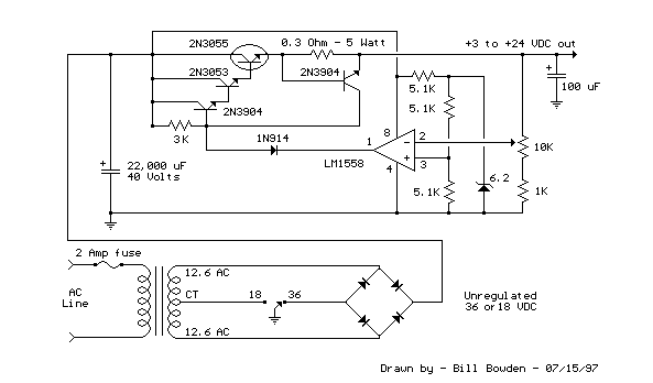
2N3055 Variable DC Power Supply circuit Diagram

Voltage range: 0.7 – 24V Current limiting range: 50mA – 2Ahttps://blogger.googleusercontent.com/img/b/R29vZ2xl/AVvXsEhhSs-ctSHZs7rS9MyKfXgLuweJsfES8qhQbGRMBR7meu51qY2tqGMCUXbH54q_Y-Vu1DHaSzoMU500UVz7lgqDC8wTjB4eQ8OTZJzpJlXZC10iLZePDiJrJPGx3yTUFRKM0EPBnYFz6eU/s800/LM1458+and+2N3055+DC+Variable+Regulator+Power+Supply.gif

A Variable DC Power Supply is one of the most useful tools on the electronics hobbyist’s workbench. This circuit is not an absolute novelty, but it is simple, reliable, “rugged” and short-proof, featuring variable voltage up to 24V and variable current limiting up to 2A. Well suited to supply the circuits shown in this website. You can adapt it to your own requirements as explained in the notes below.
Notes:

* P1 sets the maximum output current you want to be delivered by the power supply at a given output voltage.
* P2 sets the output voltage and must be a logarithmic taper type, in order to obtain a more linear scale voltage indication.
* You can choose the Transformer on the grounds of maximum voltage and current output needed. Best choices are: 36, 40 or 48V center-tapped and 50, 75, 80 or 100VA.
* Capacitor C1 can be 2200 to 6800µF, 35 to 50V.
* Q4 must be mounted on a good heatsink in order to withstand sustained output short-circuit. In some cases the rear panel of the metal box in which you will enclose the circuit can do the job.
* The 2N3055 transistor (Q4) can be replaced with the slightly less powerful TIP3055 type.

Parts:
P1____________500R Linear Potentiometer
P2_____________10K Log. Potentiometer
R1,R2___________2K2 1/2W Resistors
R3____________330R 1/4W Resistor
R4____________150R 1/4W Resistor
R5______________1R 5W Resistor
C1___________3300µF 35V Electrolytic Capacitor (see Notes)
C2______________1µF 63V Polyester Capacitor
D1,D2________1N5402 200V 3A Diodes
D3_____________5mm. Red LED
Q1____________BC182 50V 100mA NPN Transistor
Q2____________BD139 80V 1.5A NPN Transistor
Q3____________BC212 50V 100mA PNP Transistor
Q4 __________2N3055 60V 15A NPN Transistor
T1_____________220V Primary, 36V Center-tapped Secondary
50VA Mains transformer (see Notes)
PL1____________Male Mains plug
SW1____________SPST Mains switch

Read More..

Wednesday, September 24, 2014

Deriving High Current from 7805 7812 Voltage Regulator Power Supply Citcuits

  1. If, for instance, a power transistor is connected in parallel with the IC, the supply will no longer be protected against short-circuits.
  1. The circuit given here shows that a simpler solution is possible: the power transistor, T1, is provided with an emitter resistor! This effectively solves the problem, because the current through Tl is then proportional to the current supplied by the voltage regulator.
  2. But this solution A suffers from a heavy power loss during short-circuit conditions, which is not really acceptable either.
  3. There are various ways and means of drawing more current from a voltage regulator IC than it was originally intended to supply, but most methods have their disadvantages.
  4. lf the 7805 or 7812 regulator and T1 are mounted onto the same heatsink, the transistor is also thermally protected! The output voltage is dependent only on the type of voltage regulator used and, as drawn here, the circuit is suitable for currents up to 2 A.
  5. lf higher values are required, some components need to be changed according to the table. For currents above 7 A, transistor T1 must be replaced by two parallel-connected transistors each of which has an emitter resistor, R1 and R1 respectively.
  6. That can, of course, be remedied by adding a current sensor in the shape of an extra transistor which, during overload conditions, cuts off the base current to the power transistor. 
Read More..

Guitar Effect Pedal Power Circuit Diagram


A small box is fitted to the rear of the amplifier providing a 9V output for the effect pedal. The amplifier section gets 9V through a pedal switch. This power output and guitar signal input lines are combined into a single unit with multi-way cable connecting points as shown in the following figure.
Circuit diagram :
Guitar Effect Pedal Power-Circuit Diagram
Guitar Effect Pedal Power Circuit Diagram
The circuit can be divided into two sections: power supply and signal handling. The power supply section is built around transformer X1, regulators 7805 and 7905, bridge rectifier comprising diodes D1 through D4, and a few discrete components. The signal-handling circuit is built around two OP27 op-amps (IC3 and IC4). The power supply of about 9V for the effect pedals is derived from step-down transformer X1. MOV1 is a metal-oxide varistor that absorbs any large spike in mains power.  IC 7905 (IC1) is a -5V low-power regulator. By using a 3.9V zener diode (ZD1) at its ground terminal, you get -8.9V output. The same technique is also applied to IC 7805 (IC2)-a +5V regulator to get 8.9V. Use good-quality components and heat-sinks for the regulators. This supply is more than enough for the five effect pedals.
The greater the voltage drop across the regulator, the lower the output current potential. Resistors R1 and R2 provide a constant load to ensure that the regulators keep regulating. Capacitors C3 through C8 ensure that the supplies are as clean as possible. It is very important to use proper heat-sinks for IC1 and IC2. Otherwise, these could heat up.
Working of the circuit is simple. The input signal stage uses a basic differentiation amplifier to accept the incoming signal and a voltage follower to buffer the output to the power amplifier. The differential amplifier is built around IC3. It works by effectively looking at the signals presented to its inputs. If the input signals are of different amplitudes, IC3 amplifies the difference by a factor determined by R4/R3 (where R4=R6 and R3=R5). If the input signals have same amplitudes, these are attenuated by the common-mode rejection ratio (CMRR) of the circuit. The value of CMRR is determined by the choice of the op-amp the auxiliary components used and circuit topology. You can use standard resistors. With the values shown, you get an overall gain of unity.
The combination of resistor R7 and C13 serves as a passive low-pass filter, progressively attenuating unwanted high-frequency signals. The second op-amp (IC4) forms a simple voltage follower (its output follows its input), providing a low output impedance to drive into the standard power amplifier.  Assemble the circuit on a general-purpose PCB and fit it to the rear of an amplifier. The unit must be compact, yet robust. So use a very sturdy aluminium extrusion for the cabinet in order to neatly house the assembled PCB.
To ensure simple operation, there are only three connections to the unit. First, mains power is tapped from the transformer. The second lead carries the 9V output to the amplifier. The third is the guitar signal input at the five-way socket for connection to the effect pedal. 

Read More..

AB Transistor Audio Power Amplifier Circuit Diagram

This is a class AB transistor power amplifier. It is a simple amplifier to build, uses standard parts and is stable and reliable.  The entire circuit utilizes commonly available components and may be simply built over a general-purpose board. But this amplifier has very good sound quality.

There are eleven transistors, including four in the output stage. Q1 and Q2 transistor must be between 3 and 5  amperes power transistors. Q4 and Q5 must be between 100mA and 500mA driver transistors. Other transistors are 10mA small driver transistors. Q1, Q4 and Q2, Q5 are complementary pairs, they make complementary darlington pairs.

PART LIST
R11.5KΩ ¼W
R2150Ω ¼W
R31KΩ ¼W
R40.22Ω 2W
R50.22Ω 2W
R639KΩ ¼W
R71KΩ ¼W
R8120Ω ¼W
R96.8KΩ ¼W
R106.8KΩ ¼W
R1147KΩ ¼W
R1247KΩ ¼W
R132.2KΩ ¼W
R14180KΩ ¼W
R1518KΩ ¼W
C122pF Ceramic
C24.7µF 16V
C3 1000µF 25V
C4100µF 25V
D11N4148
D21N4148
 Q1 2SD313
 Q2 2SB507
 Q3 2SA733
 Q4 2SB560
 Q5 2SD400
 Q6, Q7, Q8, Q9, Q10 2SA733
 Q11 2SD400
 LS1 4Ω 20W SPEAKER
Power output of the amplifier
Supply voltage (Vs)= 20V
 Speaker impedance (R)= 4Ω
 Peak to peak voltage (Vpp)= 20-2 =18V
 Peak voltage= 9V
 Maximum output (Pmax)= 9V2/2R
= 81/8
= 10W
10W is much enough for the day today home usage.
Amplification of this amplifier (A)
A= R6/R13+1
= 39KΩ/2.2KΩ+1
= 18
Volume control can be added to the circuit by connecting a 10KΩ  POT in series to the input of the amplifier.

Q1 and Q2 must be kept sufficiently cool, so it is mounted on a suitable heat sink. If you used single heat sink please use insulation between transistors and heat sink.

Read More..

Friday, September 12, 2014

2 x 2 3 Watts power amplifier schematics

Do not misunderstand, this series is one of several series of power amplifiers that have output / low output power. This amplifier output is only possess more or less 4Watt. Or 2 X 2Watt stereo power amplifier. Minimum required voltage is not less than 3 volts and a maximum voltage of no more than 14 volts, and voltage must be rectified and filtered to obtain the maximum of the processed audio.
Low
Component List :
R1 = 2,7R
R2 = 2,7R
C1 = 1uF
C2 = 1uF
C3 = 100uF
C4 = 220uF
C5 = 100uF
C6 = 100uF
C7 = 220uF
C8 = 0.1uF
C9 = 0.1uF
C10 = 470uF
C11 = 470uF
U1 = ULN3750B
Read More..

Wednesday, September 10, 2014

Scarce Level Power Fet Driver Method Wiring diagram Schematic

This is the Scarce Level Power Fet Driver Method Circuit Diagram. This schema operates from a 16- to 50-V supply. Adding the buffer schema (within the dashed lines) offers 100-ns switching times. Otherwise, the schema switches in 1 /xs. Ql and R1 form a switched current source of about 12 mA. 

The current flows through R2, which supplies 12 V to the FET. The schema works well over a wide range of supply voltages. Furthermore, it switches smoothly in the presence of large ripple and noise on the supply. 

 Scarce Level Power Fet Driver Method Circuit Diagram


Scarce


The switching time (about 1 /as) can be reduced considerably by lowering the values of Ri and R2 at the expense of higher power dissipation in the resistors and Ql. Alternatively, a buffer schema can be added to produce switching times of 100 ns without generating significant power dissipation.
Read More..

Saturday, September 6, 2014

2x22W Stereo Power Amplifier circuit based TDA1554

This is is a stereo power amplifier schema works up to 22W on each channel. It will be 2x22W output. A few externel components required to support the main component of TDA1554. Heatsink on the power IC is a must to prevent overheating on the power IC. The chip should run cool enough to touch with the proper heatsink installed.

22W

Component part list:

R1__________39K 1/4 Watt Resistor
C1,C2_______10uf 25V Electrolytic Capacitor
C3__________100uf 25V Electrolytic Capacitor
C4__________47uf 25V Electrolytic Capacitor
C5__________0.1uf 25V Ceramic Capacitor
C6__________2200uf 25V Electrolytic Capacitor
U1__________TDA1554 Two Channel Audio Amp Chip
MISC________Heatsink For U1, Binding Posts (For Output), RCA Jacks (For Input)

Operated at 12 Volts and at about 5 Amps at full volume. Lower volumes use less current, and therefore produce less heat. Printed schema board is preferred, but universal solder or perf board will do. Keep lead length short.
Read More..

Monday, September 1, 2014

Multiple output switching power supply circuit

This power supply uses two VN400A 400 Volts  MOSFETs in a half-bridge power switch configuration. Each output consists of +5V at 20 A and 15 V at 1 A . Three-terminal regulators are used for the low-currents outputs , either 12 Volts or 15 Volts can be made available with a simple change in the transformer secondary windings. Schematic diagram below :

IC TL494 switching regulator IC provides pulse-with modulation control and drive signals for the power supply , The upper MOSFET , Q7 , in the power switch stage is driven by a simple transformer drive circuit. The lower MOSFET , Q6 , since it ground referenced , is directly driven from the control IC.
Read More..

Sunday, August 31, 2014

Power Saver Circuit Saving electricity

Power
Do you know how to work his usual power saving devices in the market is shaped like a dry battery with a plug into an outlet?. Actually you can create your own tool with much better quality with much cheaper price.


Because of the way it works is to reduce the magnitude from cosine curve AC current that will be read on the gauge kilometer. Device work if there is air conditioning load passes through a coil of wire sensors to measure the AC current which is being passed.

power
Power Saver Circuit

A very influential component in the AC circuit is a capacitor and inductor. Therefore we need to filter the AC current before it enters our home electricity network. Obviously we did not perform the act of theft of electricity, and this tool will not be detected by the device are as follows . How to installation, Here I would include a scheme of the circuit which will be installed close to the mile. The closer, the more optimal the way it works, use good quality capacitors, for security MCB here, serves to prevent the occurrence of shorting out due to damage to the capacitor. Then Enter in box or plastic box which is strong enough. Better capacitor in the cast by GIPs or cement, so that power is wasted heat well.
Read More..

Saturday, August 30, 2014

Constructing your own Dual Power Supply Rise

Many times the hobbyist desires to have a simple, dual power supply for a project. Existing power supplies may be large either in power output or physical size. a simple Dual Power Supply is necessary.For most non-critical applications the best & simplest choice for a voltage regulator is the 3-terminal type.The three terminals are input, ground & output.

The 78xx & 79xx series can provide up to 1A load current & it have on chip schemary to prevent damage in the event of over heating or excessive current. That is, the chip basically shuts down than blowing out. These regulators are cheap, simple to make use of, & they make it practical to design a method with plenty of P C Bs in which an unregulated supply is brought in & regulation is done locally on each schema board.

This Dual Power Supply project provides a dual power supply. With the appropriate choice of transformer & 3-terminal voltage regulator pairs you can basically build a tiny power supply delivering up to amp at +/- 5V, +/- 9V, +/- 12V, +/-15V or +/-18V. You require to provide the middle tapped transformer and the 3-terminal pair of regulators you require:7805 & 7905, 7809 & 7909, 7812 & 7912, 7815 & 7915or 7818 & 7918.

The user must pick the pair they needs for his particular application.

Note that the + & - regulators do not must be matched: you can for example, use a +5v & -9V pair. However,the positive regulator must be a 78xx regulator, & the negative a 79xx. They have built in plenty of safety in to this project so it ought to give plenty of years of continuous service.

Transformer
This Dual Power Supply design makes use of a full wave bridge rectifier coupled with a centre-tapped transformer. A transformer with a power output rated at at least 7VA ought to be used. The 7VA rating means that the maximum current which can be delivered without overheating will be around 390mA for the 9V+9V tap; 290mA for the 12V+12V and 230mA for the 15V+15V. If the transformer is rated by output RMS-current then the worth ought to be divided by one.2 to get the current which can be supplied. For example, in this case a 1A RMS can deliver 1/(one.2) or 830mA.

Rectifier
They use an epoxy-packaged four amp bridge rectifier with at least a peak reverse voltage of 200V. (Note the part numbers of bridge rectifiers are not standardised so the number are different from different manufacturers.) For safety the diode voltage rating ought to be at least to times that of the transformers secondary voltage. The current rating of the diodes ought to be two times the maximum load current that will be drawn.

Filter Capacitor
The purpose of the filter capacitor is to smooth out the ripple in the rectified AC voltage. Theres dual amount of ripple is determined by the worth of the filer capacitor: the larger the worth the smaller the ripple.The two,200uF is an appropriate value for all the voltages generated using this project. The other consideration in choosing the correct capacitor is its voltage rating. The working voltage of the capacitor has to be greater than the peak output voltage of the rectifier. For an 18V supply the peak output voltage is one.4 x 18V, or 25V. So they have selected a 35V rated capacitor.

Regulators
The unregulated input voltage must always be higher than the regulators output voltage by at least 3V in order for it to work. If the input/output voltage difference is greater than 3V then the excess potential must be dissipated as heat. Without a heat sink three terminal regulators can dissipate about two watts. A simple calculation of the voltage differential times the current drawn will give the watts to be dissipated. Over two watts a heat sink must be provided. If not then the regulator will automatically turn off if the internal temperature reaches 150oC. For safety it is always best to make use of a small heat sink even in case you do not think you will need.

Stability
C4 & C5 improve the regulators ability to react to sudden changes in load current & to prevent uncontrolled oscillations.

Decoupling
The mono block capacitor C2 & C6 across the output provides high frequency decoupling which keep the impedance low at high frequencies.

LED
Two LEDs are provided to show when the output regulated power is online. You do not must make use of the LEDs in the event you do not require to. However, the LED on the negative side of the schema does provide a maximum load to the 79xx regulator which they found necessary in the coursework of testing. The negative 3-pin regulators did not like a zero load situation. They have provided a 470R/0.5W resistors as the current limiting resistors for the LEDs.

Diode Protection
These protect chiefly against any back emf which may come back in to the power supply when it supplies power to inductive lots. They also provide additional short schema protection in the case that the positive output is connected by accident to the negative output. If this happened the usual current limiting shutdown in each regulator may not work as intended. The diodes will short schema in this case & protect the two regulators.

Dual Power Supply Schematic Diagram

Dual


Read More..

Wednesday, August 27, 2014

Offline Switching Power Supply Circuit 5V 10A 50W

Here the schematic diagram of offline switching power supply:

Circuit Diagram:
Offline


Parts List:
electronic

This switching power supply is using a MOSFET. For 220V AC voltage input, use BUZ80A/IXTP4N8 MOSFET and for 110V AC input voltage, use GE IRF823 MOSFET. The output will be 5 Volt DC with electric current can be reach 10A.
Read More..

Wednesday, May 29, 2013

Power Supply Monitor Using LM3914

This circuit is use to a few resistors and some LED, a simple expanded-scale voltmeter is easily constructed. Furthermore, it runs from the same single 5V ± 10% supply it monitors and can provide TTL compatible under voltage and over voltage warning signals. The complete circuit is shown in this figure.


This circuit is useful where quick and easy voltage adjustments must be made, such as in the field or on the production line. The circuit’s low cost makes it feasible to incorporate it into the system, where the overvoltage and under voltage warning signals provide an attractive extra. Of course, these techniques can be used to monitor any higher voltages, positive or negative. Calibration procedure is the LM3914 output thresholds have been shifted up by 100 mV and output #10 is or-tied with output #9. Other outputs may be wire or together if 100 mV resolution is not necessary. If desired, the outputs can be color coded by making LED #1 and LED #10 red, LED #2 and LED #9 amber, and the rest of the LEDs green to ease interpretation.

To calibrate, set VCC at 5.41V and adjust R6 until LED #9 and LED #10 are equally illuminated. (A built-in overlap of about 1 mV ensures all LEDs won’t go out at a threshold point.) There’s no need to vary the system supply voltage to perform this adjustment. Instead, disconnect R1 from VCC and connect it to an accurate reference. Then, at 4.5V, adjust R4 until LED #1 just barely turns on. There is a slight interaction caused by the finite resistance (10k, type) of the LM3914’s voltage divider, so that repeating the above procedure once is advised. The LED driver outputs can directly drive a TTL gate, so that the LED #1 and LED #10 outputs may be used for under voltage and overvoltage warning signals. These may be used to initiate a soft shutdown or summon an operator, for example. The 470Ω resistor R8 ensures that the LM3914 output will saturate to provide the proper TTL low level. Pull-up resistor R9 provides the logic high level.

Read More..

Sunday, May 26, 2013

Fuse Box BMW 733i 1982 Power Distribution Diagram

Fuse Box BMW 733i 1982 Power Distribution Diagram - Here are new post for Fuse Box BMW 733i 1982 Power Distribution Diagram.

Fuse Box BMW 733i 1982 Power Distribution Diagram


Fuse Box BMW 733i 1982 Power Distribution Diagram

Radio/Power Antenna, Radio/Power Antenna, Stoplights/Cruise Control, Warning Indicators, Rear Defogger/Sunroof, Automatic Heated Air Conditioner, Interior Lights, Lights: Turn/Hazard Warning, On Board Computer, Auxiliary Fan, Vacuum Pump, Power Window Circuit Breaker, Power Windows, Radio, Auxiliary Fan, Trunk Light, Active Check Control, Dash Lights, Gauges, Idle Speed Control, Interior Lights, Power Mirros, Power Windows, Seatbelt Warning, Speedometer, Warning Indicators, Dash Lights, Lights : Front Park/Tail/Underhood, Lights : Rear Marker/License, Backup Lights/Transmission Range, Lights, Brake Lining Warning, Cruise Control, Fuel Delivery/Evaporative Control, Idle Speed Control, Headlights, Cigar Lighters, Active Check Control, Auto Charging Flaslight., Central Locking, Gauges, Glove Box Light, Heated Door Lock, Ignition Key Warning/Seatbelt Warning, Active Check Control, Front Park/Tail, Active Check Control, Horns, Lights:Turn/Hazard Warning, Wiper/Washer, Active Check Control,
Read More..

Power Flow Studies

We will have to be capable to analyze the performance of energy techniques each in customary operating prerequisites and below fault (short-circuit) situation. The diagnosis in standard steady-state operation is referred to as an influence-flow learn about (load-flow learn about) and it goals on figuring out the voltages, currents, and actual and reactive energy floats in a device below a given load conditions.
The function of power drift studies is to plan in advance and account for various hypothetical state of affairss. For occasion, what if a transmission line throughout the power gadget properly provideing loads have to be taken off line for upkeep. Can the remaining strains within the gadget handle the desired masses without exceeding their rated parameters?

 Basic Techniques for Power-Flow Studies

A energy-flow learn about (load-flow learn about) is an prognosis of the voltages, presents, and energy go with the flows in an influence gadget under steady-state conditions. In this kind of find out about, we make an assumption about both a voltage at a bus or the ability being provided to the bus for each bus within the power gadget after which decide the magnitude and segment perspectives of the bus voltages, line currents, and so forth. that may result from the assumed aggregate of voltages and power drifts. The simplest technique to perform energy-flow calculations is by using iteration:
1. Create a bus admittance matrix Ybus for the energy system;
2. Make an initial estimate for the voltages at each and each bus in the gadget;
3. Update the voltage estimate for every bus (one at a time), in line with the estimates for the voltages and power floats at each different bus and the values of the bus admittance matrix: since the voltage at a given bus relies on the voltages at all of the other busses within the device (which are simply estimates), the up to date voltage will no longer be appropriate. However, it's going to frequently be nearer to the resolution than the unique wager.
4. Repeat this process to make the voltages at each and every bus drawing near the precise solutions closer and shut.. The equations used to update the estimates fluctuate for different sorts of busses. Each bus in an influence device will additionally be labeled to considered one of three types:
1. Load bus (PQ bus) – a buss at which the true and reactive power are specified, and for which the bus voltage will almost certainly be calculated. Real and reactive energys provided to a power device are outlined to be sure, while the abilitys consumed from the system are outlined to be bad. All busses having no mills are load busses.
2. Generator bus (PV bus) – a bus at which the magnitude of the voltage is kept consistent by way of adjusting the sector current of a synchronous generator on the bus (as we learned, increasing the box present of the generator increases each the reactive power supplied via the generator and the terminal voltage of the system). We suppose that the field present is adjusted to take care of a continuing terminal voltage VT. We also recognize that growing the top mover’s governor set factors increases the facility that generator supplies to the ability gadget. Therefore, we can keep watch over and specify the magnitude of the bus voltage and actual energy equipped.
3. Slack bus (swing bus) – a distinct generator bus serving because the reference bus for the ability machine. Its voltage is believed to be mounted in both magnitude and section (for instance, 1∠0° pu). The actual and reactive energys are uncontrolled: the bus provides no matter actual or reactive power is important to make the ability floats in the machine steadiness.
In follow, a voltage on a load bus could trade with changing hundreds. Therefore, load busses have distinct values of P and Q, while V varies with load stipulations. Real generators work most efficiently when working at full load. Therefore, it's fascinating to maintain all however one (or a few) mills working at one hundred percent capacity, while permitting the remainder (swing) generator to handle will increase and decreases in load demand. Most busses with generators will supply a set amount of power and the magnitude of their voltages will possible be deal withed steady via field circuits of turbines. These busses have specific prices of P and |Vi|.
The keep watch overs on the swing generator will most definitely be set as a lot as maintain a regular voltage and frequency, permitting P and Q to extend or decrease as masses alternate.
Read More..

Tuesday, April 30, 2013

1 5 35 Volt DC Regulated Power Supply

Here is the circuit diagram of regulated power supply. It is a small power supply that provides a regulated voltage, adjustable between 1.5 and 35 volts at 1 ampere. This circuit is ready to use, you just need to add a suitable transformer. This circuit is thermal overload protected because the current limiter and thermal overload protection are included in the IC.

Picture of the circuit:
 1A 1.5 volt to 35 volt dc Regulated Power Supply Circuit Schematic
1A Regulated Power Supply Circuit Schematic
 
Circuit diagram:
 1A 1.5 volt to 35 volt dc Regulated Power Supply Circuit Diagram
1A Regulated Power Supply Circuit Diagram
 
Transformer selection chart:
  Transformer Selection Chart for 1A 1.5 volt to 35 volt dc Regulated Power Supply Circuit Diagram
Transformer selection Guide-Table For Power Supply
 
Parts:
IC = LM317
P1 = 4.7K
R1 = 120R
C1 = 100nF - 63V
C2 = 1uF - 35V
C3 = 10uF - 35V
C4 = 2200uF - 35V
D1-D4 = 1N4007

Features:
  • Just add a suitable transformer (see table)
  • Great to power your projects and save money on batteries
  • Suitable as an adjustable power supply for experiments
  • Control DC motors, low voltage light bulbs, …
Specifications :
  • Preset any voltage between 1.5 and 35V
  • Very low ripple (80dB rejection)
  • Short-circuit, thermal and overload protection
  • Max input voltage : 28VAC or 40VDC
  • Max dissipation : 15W (with heatsink)
  • Dimensions : 52x52mm (2.1” x 2.1”)
Technical Specifications
  • Input Voltage = 40Vdc max Transformer
  • Output Voltage = 1.5V to 35Vdc
  • Output Current = 1.5 Amps max.
  • Power Dissipation = 15W max (cooled)
Note:
  • It has not to be cooled if used for small powers. 28 Volt AC max is allowed for the input voltage.
Read More..